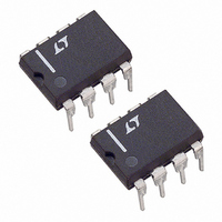
LTC1041CN8 Linear Technology, LTC1041CN8 Datasheet - Page 2

LTC1041CN8
Manufacturer Part Number
LTC1041CN8
Description
IC BANG-BANG CONTROLLER 8DIP
Manufacturer
Linear Technology
Datasheet
1.LTC1041CN8PBF.pdf
(8 pages)
Specifications of LTC1041CN8
Applications
Bang-Bang Controller
Voltage - Supply
2.8 V ~ 16 V
Current - Supply
1.2mA
Operating Temperature
-40°C ~ 85°C
Mounting Type
Through Hole
Package / Case
8-DIP (0.300", 7.62mm)
Lead Free Status / RoHS Status
Contains lead / RoHS non-compliant
Voltage - Input
-
Available stocks
Company
Part Number
Manufacturer
Quantity
Price
Company:
Part Number:
LTC1041CN8
Manufacturer:
LT
Quantity:
5 510
Company:
Part Number:
LTC1041CN8
Manufacturer:
SIEMENS
Quantity:
5 510
Part Number:
LTC1041CN8
Manufacturer:
LT
Quantity:
20 000
Company:
Part Number:
LTC1041CN8#PBF
Manufacturer:
LTC
Quantity:
400
ABSOLUTE AXI U RATI GS
(Note 1)
LTC1041
Total Supply Voltage (V
Input Voltage ........................ (V
Operating Temperature Range
Storage Temperature Range ................. – 55 C to 150 C
Lead Temperature (Soldering, 10 sec).................. 300 C
Output Short Circuit Duration ....................... Continuous
ELECTRICAL CHARACTERISTICS
temperature range, otherwise specifications are at T
SYMBOL
I
R
P
I
I
t
V
V
R
f
Note 1: Absolute Maximum Ratings are those values beyond which the life
of a device may be impaired.
2
OS
S(ON)
S(OFF)
D
S
SR
OH
OL
IN
EXT
LTC1041C ......................................... –40 C to 85 C
LTC1041M (OBSOLETE) .................. – 55 C to125 C
PARAMETER
SET POINT Error (Note 3)
Deadband Error (Note 4)
Input Current
Equivalent Input Resistance
Input Voltage Range
Power Supply Range
Power Supply ON
Current (Note 6)
Power Supply OFF
Current (Note 6)
Response Time (Note 7)
ON/OFF Output (Note 8)
Logical “1” Output Voltage
Logical “0” Output Voltage
External Timing Resistor
Sampling Frequency
W
+
to V
W W
–
) .............................. 18V
+
+ 0.3V) to (V
CONDITIONS
V
V
V
V
V
(V
f
V
V
V
V
V
Resistor Connected between V
V
R
S
EXT
+
+
+
+
+
+
+
+
+
+
+
IN
= 1kHz (Note 5)
= 2.8V to 6V (Note 2)
= 6V to 15V (Note 2)
= 2.8V to 6V (Note 2)
= 6V to 15V (Note 2)
= 5V, T
= 5V, V
= 5V, V
= 5V
= 4.75V, I
= 4.75V, I
= 5V, T
, SET POINT and DELTA Inputs)
= 1M C
A
A
P-P
P-P
U
= 25 C, OSC = GND
= 25 C,
EXT
OUT
OUT
OFF
A
ON
= 25 C. Test Conditions: V
–
= 0.1 F
= –360 A
= 1.6mA
– 0.3V)
The denotes the specifications which apply over the full operating
LTC1041C
LTC1041M
+
and OSC Pin
PACKAGE/ORDER I FOR ATIO
Consult LTC Marketing for parts specified with wider operating temperature ranges.
Note 2: Applies over input voltage range limit and includes gain
uncertainty.
SET POINT
ON / OFF
Consider the N8 Package as an Alternate Source
OBSOLETE PACKAGE
GND
N8 PACKAGE
8-LEAD PDIP
V
T
T
IN
JMAX
JMAX
T
+
JMAX
= 5V, unless otherwise specified.
1
2
3
4
= 110 C,
= 150 C,
= 150 C,
8-LEAD CERDIP
J8 PACKAGE
TOP VIEW
JA
JA
MIN
GND
100
2.8
2.4
10
60
JA
= 150 C/W (N8)
= 150 C/W (S8)
= 100 C/W
S8 PACKAGE
8-LEAD PDIP
TC1041M/LTC1041C
8
7
6
5
V
V
OSC
DELTA
0.001
0.001
+
P-P
TYP
0.25
0.05
0.05
1.2
4.4
15
80
0.3
+
0.6
+
0.1
+
0.1
0.3
5
+
1
2
U
10,000
MAX
ORDER PART
LTC1041CN8
W
LTC1041CS8
LTC1041MJ8
0.5
100
V
0.4
16
0.5
0.1
0.1
0.2
0.2
5
+
+
+
+
3
1
6
3
+
NUMBER
% of DELTA
% of DELTA
% of DELTA
% of DELTA
UNITS
U
1041fa
M
mV
mV
mV
mA
k
nA
Hz
V
V
A
A
V
V
s


