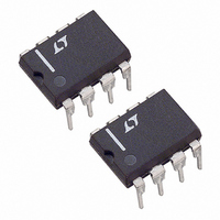
LTC1041CN8 Linear Technology, LTC1041CN8 Datasheet - Page 6

LTC1041CN8
Manufacturer Part Number
LTC1041CN8
Description
IC BANG-BANG CONTROLLER 8DIP
Manufacturer
Linear Technology
Datasheet
1.LTC1041CN8PBF.pdf
(8 pages)
Specifications of LTC1041CN8
Applications
Bang-Bang Controller
Voltage - Supply
2.8 V ~ 16 V
Current - Supply
1.2mA
Operating Temperature
-40°C ~ 85°C
Mounting Type
Through Hole
Package / Case
8-DIP (0.300", 7.62mm)
Lead Free Status / RoHS Status
Contains lead / RoHS non-compliant
Voltage - Input
-
Available stocks
Company
Part Number
Manufacturer
Quantity
Price
Company:
Part Number:
LTC1041CN8
Manufacturer:
LT
Quantity:
5 510
Company:
Part Number:
LTC1041CN8
Manufacturer:
SIEMENS
Quantity:
5 510
Part Number:
LTC1041CN8
Manufacturer:
LT
Quantity:
20 000
Company:
Part Number:
LTC1041CN8#PBF
Manufacturer:
LTC
Quantity:
400
LTC1041
If the best possible performance is needed, the inputs to
the LTC1041 must completely settle within 4 s of the start
of the comparison cycle (V
transition). Also, it is critical that the input voltages do not
change during the 80 s active time. When driving resistive
input networks with V
minimized to meet the 4 s settling time requirement.
Further, care should be exercised in layout when driving
networks with source impedances, as seen by the LTC1041,
of greater than 10k (see For R
APPLICATIO S I FOR ATIO
6
LT1009-2.5
R1
R2
Figure 5. Driving Reference with V
Figure 4. Ratiometric Network Driven by V
COMPARATOR ON TIME
R3
R4
R1
80 s
Figure 3. V
I
L
R5
R6
U
R2
R3
R4
SET POINT
P-P
V
IN
P-P
SET POINT
U
, capacitive loading should be
GND
4
Output Switch
P-P
GND
V
1
2
3
4
IN
S
high impedance to V
1
2
3
4
> 10k ).
V
Q1
8
W
+
LTC1041
V
LTC1041
7
P-P
P1
P-P
Output
LTC1041 • AI03
8
7
6
5
P-P
LTC1041 • AI05
U
DELTA
8
7
6
5
LTC1041 • AI04
V
+
V
DELTA
V
P-P
+
+
In applications where an absolute reference is required,
the V
reference. The LTC1009 2.5V reference settles in
and is ideal for this application (Figure 5). The current
through R1 must be large enough to supply the LT1009
minimum bias current ( 1mA) and the load current, I
Internal Oscillator
An internal oscillator allows the LTC1041 to strobe itself.
The frequency of the oscillation, and hence the sampling
rate, is set with an external RC network (see typical curve,
Sampling Rate R
as shown in Figure 1. To assure oscillation, R
between 100k and 10M . There is no limit to the size of
C
At low sampling rates, R
determining the power consumption. R
power continuously. The average voltage at the OSC pin
is approximately V
P
Example: assume R
(2.5)
power consumed by the LTC1041 at V
f
R
power dissipated by R
If high sampling rates are needed and power consumption
is of secondary importance, a convenient way to get the
maximum possible sampling rate is to make R
and C
active time, will nominally be 10kHz.
To synchronize the Sampling of the LTC1041 to an
external frequency source, the OSC pin can be driven by a
CMOS gate. A CMOS gate is necessary because the input
trip points of the oscillator are close to the supply rails and
TTL does not have enough output swing. Externally driven,
there will be a delay from the rising edge of the OSC input
and the start of the sampling cycle of approximately 5 s.
S
EXT
REXT
EXT
= 1 sample/second. Where power is a premium,
.
2
should be made as large as possible. Note that the
P-P
EXT
/10
= (V
6
= 0. The sampling rate, set by the controller’s
output can be used to drive a fast settling
= 6.25/ W. This is approximately four times the
+
/ 2)
2
/R
EXT
EXT
, C
+
/2, giving a power dissipation of
.
EXT
EXT
EXT
). R
is not a function of f
= 1M , V
EXT
EXT
and C
is very important in
+
EXT
= 5V, P
EXT
are connected
+
EXT
EXT
= 5V and
consumes
S
or C
= 100k
must be
REXT
EXT
1041fa
2 s
L
.
=
.


