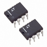
LTC1041CN8 Linear Technology, LTC1041CN8 Datasheet - Page 5

LTC1041CN8
Manufacturer Part Number
LTC1041CN8
Description
IC BANG-BANG CONTROLLER 8DIP
Manufacturer
Linear Technology
Datasheet
1.LTC1041CN8PBF.pdf
(8 pages)
Specifications of LTC1041CN8
Applications
Bang-Bang Controller
Voltage - Supply
2.8 V ~ 16 V
Current - Supply
1.2mA
Operating Temperature
-40°C ~ 85°C
Mounting Type
Through Hole
Package / Case
8-DIP (0.300", 7.62mm)
Lead Free Status / RoHS Status
Contains lead / RoHS non-compliant
Voltage - Input
-
Available stocks
Company
Part Number
Manufacturer
Quantity
Price
Company:
Part Number:
LTC1041CN8
Manufacturer:
LT
Quantity:
5 510
Company:
Part Number:
LTC1041CN8
Manufacturer:
SIEMENS
Quantity:
5 510
Part Number:
LTC1041CN8
Manufacturer:
LT
Quantity:
20 000
Company:
Part Number:
LTC1041CN8#PBF
Manufacturer:
LTC
Quantity:
400
APPLICATIO S I FOR ATIO
R
source during the controller’s active time is critical in
determining errors caused by the input charging current.
For source resistances less than 10k , C
and no error is caused by the charging current.
For R
For source resistances greater than 10k , C
charge, causing voltage errors. To minimize these errors,
an input bypass capacitor, C
shared between C
The magnitude of this error is A
error can be made arbitrarily small by increasing C
The averaging effect of the bypass capacitor, C
another error term. Each time the input switches cycle
between the plus and minus inputs, C
discharged. The average input current due to this is
I
Because the input current is directly proportional to the
differential input voltage, the LTC1041 can be said to have
an average input resistance of R
Since two comparator inputs are connected in parallel, R
is one half of this value (see typical curve of R
Sampling Frequency). This finite input resistance causes
an error due to the voltage divider between R
The input voltage error caused by both of these effects is
V
Example: assume f
V
the error is caused by R
reduced to 1Hz, the voltage error from the input
impedance effects is reduced to 136 V.
AVG
ERROR
ERROR
S
• C
= V
S
IN
> 10k
= 1V(66 V + 660 V) = 726 V. Notice that most of
= V
IN
. The ability to fully charge C
V
IN
R
• C
S
IN
IN
[2C
Figure 2. Equivalent Input Circuit
• f
C
IN
IN
S
S
S
/(2C
, where f
U
and C
+
–
= 10Hz, R
IN
IN
S1
S2
S
U
LTC1041 DIFFERENTIAL INPUT
+ C
, causing a small voltage error.
. If the sampling frequency is
S
S
S
, should be used. Charge is
is the sampling frequency.
S
V
) + R
IN
= V
= 1M, C
= V
IN
W
S
/(R
IN
V
• C
–
IN
/I
IN
S
( 33pF)
IN
S
AVG
from the signal
= 1 F, V
C
IN
is charged and
+ R
(C
IN
IN
fully charges
IN
= I/(f
LTC1041 • AI01
IN
cannot fully
S
+ C
U
)].
S
and R
IN
, causes
S
IN
S
versus
). This
• C
S
= 1V,
.
IN
IN
IN
.
).
Input Voltage Range
The input switches of the LTC1041 are capable of
switching either to the V
the input voltage range includes both supply rails. This is
a further benefit of the sampling input structure.
Error Specifications
The only measurable errors on the LTC1041 are the
deviations from “ideal” of the upper and lower switching
levels (Figure 1b). From a control standpoint, the error in
the SET POINT and deadband is critical. These errors may
be defined in terms of V
The specified error limits (see electrical characteristics)
include error due to offset, power supply variation, gain,
time and temperature.
Pulsed Power (V
It is often desirable to use the LTC1041 with resistive
networks such as bridges and voltage dividers. The power
consumed by these resistive networks can far exceed that
of the LTC1041 itself.
At low sample rates the LTC1041 spends most of its time
off. A switched power output, V
input network, reducing its average power as well. V
switched to V
and to a high impedance (open circuit) when internal
power is switched off.
Figure 3 shows the V
voltage is not precisely controlled when driving a load
(see typical curve of V
In spite of this, high precision can be achieved in two ways:
(1) driving ratiometric networks and (2) driving fast set-
tling references.
In ratiometric networks all the inputs are proportional to
V
does not affect accuracy.
P-P
SET POINT error
deadband error
(Figure 4). Consequently, the absolute value of V
+
during the controller’s active time ( 80 s)
P-P
) Output
P-P
P-P
+
U
Output Voltage vs Load Current).
supply or ground. Consequently,
V
output circuit. The V
V
U
and V
U
–
2
V
P-P
V
L
L
L
.
– •
, is provided to drive the
–
2
SET POINT
DELTA
LTC1041
P-P
output
P-P
1041fa
5
P-P
is


