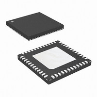
ISL6595DRZ-T Intersil, ISL6595DRZ-T Datasheet - Page 12

ISL6595DRZ-T
Manufacturer Part Number
ISL6595DRZ-T
Description
IC DIGITL MULTIPHASE CTRLR 48QFN
Manufacturer
Intersil
Datasheet
1.ISL6595DRZ-T.pdf
(22 pages)
Specifications of ISL6595DRZ-T
Applications
Digital Multiphase Controller
Voltage - Supply
3 V ~ 3.6 V
Current - Supply
100mA
Operating Temperature
0°C ~ 85°C
Mounting Type
Surface Mount
Package / Case
48-VQFN
Lead Free Status / RoHS Status
Lead free / RoHS Compliant
Voltage - Input
-
supported by the ISL6595. These are single-ended r
sense of the low-side FET, differential r
low-side FET, or differential DCR sense of the buck inductor.
The sensed current is digitized using a multiplexed current
ADC.
For low-side r
pin is held at virtual ground with a programmable offset from
25mV to 100mV. An external sense resistor is connected to
the drain of the low side FET to monitor the current in this
device. The current sourced from the input is then given in
Equation 3:
where input current is digitized with the ADC with an
effective ADC range of 0µA to 275µA in 4.3µA steps.
For DCR current sense applications, a resistor in series with
a capacitor is placed across the inductor for each phase. In
this configuration, the resistor is tied to the FET side of the
inductor while the capacitor is tied to the load side of the
inductor. If the RC values are chosen such that the RC time
constant matches the L/DCR time constant, the resultant
voltage appearing across the capacitor will equal the voltage
across the inductor series resistance and thus represent the
current flowing through the inductor. In this application, a
sense resistor is then placed from the ISENx+ pin to the load
side of the capacitor while the ISENx- pin in placed on the
FET side of the capacitor. The current sourced from the input
is then given in Equation 4:
where Input current is digitized with the ADC with an
effective ADC range of 0µA to 275µA in 4.3µA steps.
Differential r
The positive current sense inputs (ISEN1+ to ISEN6+) are
held at a virtual ground with a programmable offset from
25mV to 100mV, in 25mV steps. The negative current sense
inputs (ISEN1- to ISEN6-) should be tied to the ground plane
local to the low side FET being sensed to eliminate the
effects of ground differences between the FET and the
ISL6595. The large voltage swing at the drain of the low side
FET is eliminated by using a series resistor, converting the
signal to a current equal to that in Equation 5:
where I
Voffset is the programmable offset, V
across the low side FET, and R
whose value is chosen to scale the input depending on the
expected r
The input current is mirrored and multiplexed, then digitized
by the 6-bit current ADC with an effective input range of
ISEN
ISEN
ISENSE
=
=
SENSE
(
---------------------------------------------------------------- -
(
----------------------------------------------------- -
V
V
=
DS(ON)
OFFSET
OFFSET
(
------------------------------------------------ -
V
DS(ON)
OFFSET
DS(ON)
is the current sourced by the sense input,
R
R
R
SEN
SENSE
.
SEN1
–
–
Vr
V
current sense applications, the ISENx+
DCR
–
DS ON
Current Sense
V
DS
(
)
)
12
)
)
SENSE
DS
is an external resistor
DS(ON)
is the voltage
sense of the
DS(ON)
(EQ. 3)
(EQ. 4)
(EQ. 5)
ISL6595
0µA to 275µA in 4.3µA steps. The ADC samples the current
in each phase once per switching cycle, and the sampling
instant can be varied using a programmable delay, such that
sampling in the middle of the ON-cycle can be guaranteed.
The current in the power stage can then be inferred from the
current ADC measurement if the drain-source resistance
(r
can be either programmed as a default value, or it can be
determined by running the calibration routine either one time
at system test or every time the system starts up. Calibration
is performed by providing a known current load while the
regulator is on and correcting the gain and offset of the
current measurement. This requires the use of a precision
external current source consisting of a dedicated calibration
FET and sense resistor. The ISL6595 senses the voltage
across the resistor and provides a variable voltage to drive
the gate of the calibration FET, varying its r
the current through the FET and resistor are under closed
loop control. The calibration current and voltage level at
which calibration occurs are programmable, and the
calibration routine can be bypassed if the default values are
to be used. The r
temperature drift using either the on-chip temperature sense
or an external thermistor that can be placed close to the
power stage.
Differential DCR Current Sense
For DCR current sense applications, a resistor in series with
a capacitor is placed across the inductor for each phase. In
this configuration, the resistor is tied to the FET side of the
inductor while the capacitor is tied to the load side of the
inductor. If the RC values are chosen such that the RC time
constant matches the L/DCR time constant, the resultant
voltage appearing across the capacitor will equal the voltage
across the inductor series resistance and thus represent the
current flowing through the inductor. In this application, a
sense resistor is then placed from the ISENX+ pin to the
load side of the capacitor while the ISENX- pin in placed on
the FET side of the capacitor. The current sourced from the
input is then given in Equation 6:
where input current is digitized with the ADC with an
effective ADC range of 0µA to 275µA in 4.3µA steps.
ISEN
DS(ON)
=
) of the FET is known. The r
(
----------------------------------------------------- -
V
OFFSET
R
SENSE
DS(ON)
–
V
DCR
value is compensated for
)
DS(ON)
DS(ON)
of each FET
December 4, 2008
such that
FN9192.2
(EQ. 6)


