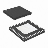
ISL6595DRZ Intersil, ISL6595DRZ Datasheet - Page 13

ISL6595DRZ
Manufacturer Part Number
ISL6595DRZ
Description
IC DIGITL MULTIPHASE CTRLR 48QFN
Manufacturer
Intersil
Datasheet
1.ISL6595DRZ-T.pdf
(22 pages)
Specifications of ISL6595DRZ
Applications
Digital Multiphase Controller
Voltage - Supply
3 V ~ 3.6 V
Current - Supply
100mA
Operating Temperature
0°C ~ 85°C
Mounting Type
Surface Mount
Package / Case
48-VQFN
Lead Free Status / RoHS Status
Lead free / RoHS Compliant
Voltage - Input
-
External Temperature Sense
When configured to sense temperature from an external
thermistor, the temperature sense input, TEMP_SEN, is set
at virtual ground with a fixed offset of 300mV. An external
negative TC thermistor is tied to ground, generating the input
current for the measurement. A series and shunt resistor
network should be used to scale the resultant current to the
proper range. The current range is the same as the current
sense inputs, from 0µA to 275µA in 4.3µA steps.
The ADC measurements are converted to temperature using
a programmable 4-segment piece-wise linear table while the
internal proportional-to-absolute temperature (PTAT)
reference is digitized directly, using a linear curve fit. Both
internal and external temperature measurements are
multiplexed through the current ADC at a low frequency,
providing run-time internal and external temperature
information to perform temperature compensation, reporting,
alerts and shutdown.
Digital Control Loop and PWM Generation
The digital control loop uses a proportional, integral, and
derivative (PID) compensator to drive the digitized sense
voltage to the desired target. An additional second
derivative gain term and a 2
additional high order zeros and poles to further refine the
wideband characteristics of the loop. All loop parameters are
programmable over a wide range of values, allowing loop
bandwidths of 10kHz to 300kHz to be attained depending on
the number and type of power stages used.
PWM
FIGURE 4. DIFFERENTIAL DCR SENSE
PWM
ISL6594
ADC
ISL6595
VIN
nd
13
order post-filter provide
ISEN-
ISEN+
VOUT
ISL6595
The effective transfer function of the compensator is given
by Equation 7:
where:
The control loop operates at the same frequency as the
voltage ADC, which is synchronous to the switching
frequency and given by Equation 8:
The compensator digital output is converted to a pulse width
using a digital counter based pulse width modulator. The
pulse width modulator uses two successive samples to
modulate the leading edge and then the trailing edge of a
pulse. The modulator provides for monotonic edge
placements with a resolution of 100ps. The next two
samples are then used to modulate the next phase in the
firing sequence. The pulse width modulator is capable of
setting a maximum duty cycle limit, overlapping adjacent
phases, a minimum pulse width of 13ns, and also producing
zero pulse width with minimal glitching.
Voltage Identification Codes
The target voltage is provided by external parallel 8-bit
voltage identification (VID) inputs. The ISL6595 is fully
compliant with VRD/VRM 11.0 deglitching and dynamic VID
stepping requirements.
H z ( )
⎛
⎜
⎝
F
--------------------------------------------------------- -
1
S
+
K
derivative, and second derivative gain terms
K
pole low pass post-filter
K
term
N
ratio setting the switching frequency
V
Q is the ADC step size, 3.125mV
(
1
=
K
i
fd1
mod
ph
IN
, K
=
+
fd1
2 ∗ Nph*fsw
is the power stage input voltage, typically 12V
K
⎛
⎜
⎝
is the number of phases and div_sel is the divider
p
z
and K
----------------- -
1 z
fd1
, K
–
is a programmable maximum duty cycle scaling
–
1
K
d
+
+
i
–
, and K
K
K
1
fd2
fd2
fd1
+
K
z
are the coefficients of a second order all
=
)
p
–
2
156.25MHz/div_sel
+
d2
⎞
⎟
⎠
K
⎛
⎜
⎝
---------------------------------- -
N
d
are the integral, proportional,
(
ph
(
1 z
K
⋅
–
mod
div_sel
–
1
)
+
⎞ V
⎟
⎠
K
⎛
⎝
d2
---------
Q
IN
(
1 z
⎞
⎠
–
–
1
)
2
)
December 4, 2008
⎞
⎟
⎠
FN9192.2
(EQ. 7)
(EQ. 8)


