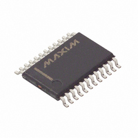
DS1780E Maxim Integrated Products, DS1780E Datasheet - Page 10

DS1780E
Manufacturer Part Number
DS1780E
Description
IC CPU PERIPHERAL MON 24-TSSOP
Manufacturer
Maxim Integrated Products
Datasheet
1.DS1780E.pdf
(28 pages)
Specifications of DS1780E
Function
Thermal Monitor, CPU Peripherals
Topology
ADC (Sigma Delta), Comparator, Fan Speed Control, Register Bank
Sensor Type
Internal
Sensing Temperature
-40°C ~ 125°C
Output Type
I²C™/SMBus™
Output Alarm
No
Output Fan
Yes
Voltage - Supply
2.8 V ~ 5.75 V
Operating Temperature
-40°C ~ 125°C
Mounting Type
Surface Mount
Package / Case
24-TSSOP
Full Temp Accuracy
+/- 12 %
Digital Output - Bus Interface
Serial (2-Wire)
Digital Output - Number Of Bits
8 bit
Maximum Operating Temperature
+ 125 C
Minimum Operating Temperature
- 40 C
Lead Free Status / RoHS Status
Contains lead / RoHS non-compliant
Available stocks
Company
Part Number
Manufacturer
Quantity
Price
Company:
Part Number:
DS1780E
Manufacturer:
MAX
Quantity:
3 000
Part Number:
DS1780E
Manufacturer:
DALLAS
Quantity:
20 000
Part Number:
DS1780E+T&R
Manufacturer:
MAXIM/美信
Quantity:
20 000
Company:
Part Number:
DS1780E+TR
Manufacturer:
MAXIM
Quantity:
1 001
Company:
Part Number:
DS1780E-TR
Manufacturer:
ICS
Quantity:
933
Company:
Part Number:
DS1780E/TR
Manufacturer:
XILINX
Quantity:
17
V
V
If the +2.5V
removed and R1=500Ω. Table 6 below shows the voltage/data relationship for these inputs in the ideal
case. In this example, V
Analog inputs will provide best accuracy when referred to the GNDA pin. A separate, low-impedance
ground plane for analog ground, which provides a ground point for the voltage dividers and analog
components will provide best performance but is not mandatory. Analog components such as voltage
dividers should be located physically as close as possible to the DS1780.
The power supply bypass, the parallel combination of 10 µF (electrolytic or tantalum) and 0.1 µF
(ceramic) bypass capacitors connected between pin 9 and ground, should also be located as close as
possible to the DS1780.
VOLTAGE/DATA RELATIONSHIPS FOR V
(+V
OPERATION - FAN Speed Data Format
Inputs are provided for signals from fans equipped with tachometer outputs. These are logic-level inputs
with an approximate threshold of 1.4V. Signal conditioning in the DS1780 accommodates the slow rise
and fall times typical of fan tachometer outputs. The maximum input signal range is 0 to V
event these inputs are supplied from fan outputs which exceed 0 to V
clamping must be included to keep inputs within an acceptable range, as shown in Figure 3. R2 is
selected so that it does not develop excessive voltage due to input leakage. R1 is selected based on R2 to
provide a minimum input of 2V and a maximum of V
MIN
MAX
CCP1
(V
(V
ADC RESULT (BASE 10)
LSb WEIGHTING (mV)
REF
REF
, +2.5VS/ +V
, R
, R
S
INPUT PIN
/+V
1
1
, R
, R
136
137
138
139
252
253
254
255
CCP2
0
1
2
3
4
•
•
•
•
•
•
2
2
) @ -
) @ V
is to be used to monitor a secondary processor core voltage (V
R
R
REF
REF
2
1
CCP2
V
=+5.0V, R1=4.0 kΩ, and R2=23.2 kΩ.
-(V
REF
) Table 6
REF
-3.6)
é
ê
ë
R
1
R
+
(Used to monitor V
1
R
PIN VOLTAGE (V)
2
ù
ú
û
10 of 28
+V
0.014
0.028
0.042
0.056
1.920
1.934
1.948
1.962
3.558
3.572
3.586
14.1
3.60
0
CCP1
•
•
•
•
•
•
DD
CCP
. R1 should be as low as possible to provide the
CCP
VOLTAGE INPUTS
)
DD
, either resistive division or diode
SUPPLY VOLTAGE (V)
(Used to monitor -12V)
+2.5V
CCP2
-28.90
-28.81
-28.71
-28.62
-15.94
-15.85
-15.75
-15.66
-4.808
-4.712
-4.616
-29.0
-4.52
96.0
S
/+V
•
•
•
•
•
•
), R2 should be
CCP2
DD
. In the


