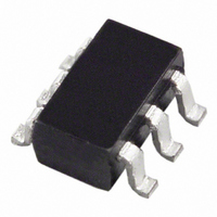
ADR127AUJZ-R2 Analog Devices Inc, ADR127AUJZ-R2 Datasheet - Page 17

ADR127AUJZ-R2
Manufacturer Part Number
ADR127AUJZ-R2
Description
IC V-REF PREC 1.25V TSOT-23-6
Manufacturer
Analog Devices Inc
Datasheet
1.ADR127AUJZ-REEL7.pdf
(20 pages)
Specifications of ADR127AUJZ-R2
Temperature Coefficient
25ppm/°C
Design Resources
Generating a Negative Precision Voltage Reference Without Precision Resistors (CN0005) Single Supply Low Noise LED Current Source Driver Using a Current Output DAC in the Reverse Mode (CN0139)
Reference Type
Series
Voltage - Output
1.25V
Tolerance
±0.24%
Voltage - Input
2.7 ~ 18 V
Number Of Channels
1
Current - Quiescent
95µA
Current - Output
5mA
Operating Temperature
-40°C ~ 125°C
Mounting Type
Surface Mount
Package / Case
TSOT-23-6, TSOT-6
Topology
Series
Input Voltage
2.7V To 18V
Reference Voltage
1.25V
Reference Voltage Tolerance
3mV
Voltage Reference Case Style
TSOT
No. Of Pins
6
Lead Free Status / RoHS Status
Lead free / RoHS Compliant
Current - Cathode
-
Lead Free Status / RoHS Status
Lead free / RoHS Compliant, Lead free / RoHS Compliant
APPLICATIONS INFORMATION
BASIC VOLTAGE REFERENCE CONNECTION
The circuit in Figure 49 illustrates the basic configuration for
the ADR12x family voltage reference.
STACKING REFERENCE ICs FOR ARBITRARY
OUTPUTS
Some applications may require two reference voltage sources
that are a combined sum of the standard outputs. Figure 50
shows how this stacked output reference can be implemented.
Two reference ICs are used and fed from an unregulated input,
V
which provides two output voltages, V
the terminal voltage of U1, whereas V
voltage and the terminal of U2. U1 and U2 are chosen for the
two voltages that supply the required outputs (see Table 6). For
example, if U1 and U2 are ADR127s and V
1.25 V and V
IN
. The outputs of the individual ICs are connected in series,
V
IN
Figure 49. Basic Configuration for the ADR12x Family
Figure 50. Stacking References with the ADR12x
OUT2
INPUT
0.1µF
is 2.5 V.
+
0.1µF
1
2
3
0.1µF
NC
GND
V
IN
ADR12x
1
2
3
1
2
3
NC
GND
V
NC
GND
V
IN
IN
V
ADR12x
ADR12x
OUT
NC
NC
U2
U1
6
5
4
OUT2
OUT1
V
V
OUT
OUT
NC
NC
NC
NC
+
0.1µF
is the sum of this
and V
OUTPUT
IN
6
5
4
6
5
4
≥ 3.95 V, V
OUT2
V
V
0.1µF
0.1µF
. V
OUT2
OUT1
OUT1
OUT1
is
Rev. B | Page 17 of 20
is
Table 6. Required Outputs
U1/U2
ADR127/ADR121
ADR127/ADR125
ADR121/ADR125
NEGATIVE PRECISION REFERENCE WITHOUT
PRECISION RESISTORS
A negative reference is easily generated by adding an op
amp, for example, the AD8603, and is configured as shown in
Figure 51. V
reference can be taken directly from the output of the op amp.
The op amp must be dual-supply, low offset, and rail-to-rail if
the negative supply voltage is close to the reference output.
GENERAL-PURPOSE CURRENT SOURCE
In low power applications, the need can arise for a precision
current source that can operate on low supply voltages. The
ADR12x can be configured as a precision current source (see
Figure 52). The circuit configuration shown is a floating current
source with a grounded load. The reference’s output voltage is
bootstrapped across R
load. With this configuration, circuit precision is maintained for
load currents ranging from the reference’s supply current, typi-
cally 85 μA, to approximately 5 mA.
OUT
–V
+V
+V
REF
DD
DD
is at virtual ground and, therefore, the negative
Figure 52. ADR12x Trim Configuration
Figure 51. Negative Reference
SET
1
2
3
ADR121/ADR125/ADR127
, which sets the output current into the
NC
GND
V
IN
ADR12x
AD8603
1
2
3
–V
I
SY
NC
GND
V
V+
V–
DD
IN
ADR127
V
–
+
OUT
1.25 V
1.25 V
2.5 V
V
NC
NC
OUT2
2
3
0.1µF
R
6
5
4
SET
V
R
OUT
L
NC
NC
1kΩ
P1
6
5
4
I
SET
3.75 V
6.25 V
7.5 V
V
OUT1


