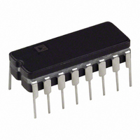
AD688BQ Analog Devices Inc, AD688BQ Datasheet - Page 11

AD688BQ
Manufacturer Part Number
AD688BQ
Description
IC VREF HIGH PREC +/-10V 16-CDIP
Manufacturer
Analog Devices Inc
Datasheet
1.AD688AQ.pdf
(16 pages)
Specifications of AD688BQ
Temperature Coefficient
3ppm/°C
Rohs Status
RoHS non-compliant
Reference Type
Series
Voltage - Output
±10V
Tolerance
±2mV
Number Of Channels
2
Current - Quiescent
12mA
Current - Output
10mA
Operating Temperature
-40°C ~ 85°C
Mounting Type
Through Hole
Package / Case
16-CDIP (0.300", 7.62mm)
Topology
Series
Input Voltage
12V To 36V
Reference Voltage
10V
Reference Voltage Tolerance
2mV
Voltage Reference Case Style
DIP
No. Of Pins
16
Voltage - Input
-
Current - Cathode
-
Lead Free Status / RoHS Status
Contains lead / RoHS non-compliant
Available stocks
Company
Part Number
Manufacturer
Quantity
Price
Part Number:
AD688BQ
Manufacturer:
ADI/亚德诺
Quantity:
20 000
DYNAMIC PERFORMANCE
The output buffer amplifiers (A3 and A4) are designed to
provide the AD688 with static and dynamic load regulation
superior to less complete references.
Many A/D and D/A converters present transient current loads
to the reference, and poor reference response can degrade the
converter’s performance.
Figure 20, Figure 21, and Figure 22 display the characteristic of
the AD688 output amplifier driving a 0 mA to 10 mA load.
Figure 23 and Figure 24 display the output amplifier
characteristic driving a 5 mA to 10 mA load, a common
situation found when the reference is shared among multiple
converters or is used to provide bipolar offset current.
V
V
OUT
OUT
V
V
L
L
100
90
10
100
90
10
0%
Figure 22. Fine-Scale Settling for Transient Load
Figure 21. Large-Scale Transient Response
1mV
200mV
Figure 20. Transient Load Test Circuit
10V
A3 OR A4
5V
5V
V
I
L
L
1kΩ
10V
0V
V
OUT
2µs
500ns
Rev. B | Page 11 of 16
In some applications, a varying load may be both resistive and
capacitive in nature, or may be connected to the AD688 by a
long capacitive cable. Figure 25 and Figure 26 display the output
amplifier characteristics driving a 1000 pF, 0 mA to 10 mA load.
Figure 27 and Figure 28 display the crosstalk between output
amplifiers. The top trace shows the output of A4, dc-coupled
and offset by 10 V, while the output of A3 is subjected to a 0 mA
to 10 mA load current step. The transient at A4 settles in about
1 µs, and the load-induced offset is about 100 µV.
1mV/CM
200mV/
C
1000pF
C
L
V
V
L
=
OUT
OUT
CM
= 0
V
V
Figure 25. Capacitive Load Transient Response Test Circuit
L
L
100
90
10
0%
Figure 23. Transient and Constant Load Test Circuit
100
90
10
0%
Figure 24. Transient Response 5 mA to 10 mA Load
Figure 26. Output Response with Capacitive Load
1mV
200mV
10V
10V
+
–
A3 OR A4
5V
5V
200mV
1000pF
C
V
I
L
L
L
2k Ω
10V
0V
V
L
2k Ω
1kΩ
10V
0V
V
V
OUT
OUT
1µs
1µs
AD688


