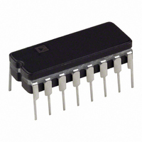
AD688BQ Analog Devices Inc, AD688BQ Datasheet - Page 6

AD688BQ
Manufacturer Part Number
AD688BQ
Description
IC VREF HIGH PREC +/-10V 16-CDIP
Manufacturer
Analog Devices Inc
Datasheet
1.AD688AQ.pdf
(16 pages)
Specifications of AD688BQ
Temperature Coefficient
3ppm/°C
Rohs Status
RoHS non-compliant
Reference Type
Series
Voltage - Output
±10V
Tolerance
±2mV
Number Of Channels
2
Current - Quiescent
12mA
Current - Output
10mA
Operating Temperature
-40°C ~ 85°C
Mounting Type
Through Hole
Package / Case
16-CDIP (0.300", 7.62mm)
Topology
Series
Input Voltage
12V To 36V
Reference Voltage
10V
Reference Voltage Tolerance
2mV
Voltage Reference Case Style
DIP
No. Of Pins
16
Voltage - Input
-
Current - Cathode
-
Lead Free Status / RoHS Status
Contains lead / RoHS non-compliant
Available stocks
Company
Part Number
Manufacturer
Quantity
Price
Part Number:
AD688BQ
Manufacturer:
ADI/亚德诺
Quantity:
20 000
AD688
THEORY OF OPERATION
The AD688 consists of a buried Zener diode reference,
amplifiers and associated thin-film resistors as shown in
Figure 3. The temperature compensation circuitry provides the
device with a temperature coefficient of 1.5 ppm/°C or less.
Amplifier A1 performs several functions. A1 primarily acts to
amplify the Zener voltage to the required 20 V. In addition, A1
also provides for external adjustment of the 20 V output
through Pin 5 (GAIN ADJ). Using the bias compensation
resistor between the Zener output and the noninverting input to
A1, a capacitor can be added at the noise reduction pin (Pin 7)
to form a low-pass filter and reduce the noise contribution of
the Zener to the circuit. Two matched 12 kΩ nominal thin-film
resistors (R4 and R5) divide the 20 V output in half.
Ground sensing for the circuit is provided by amplifier A2. The
noninverting input (Pin 9) senses the system ground and forces
the midpoint of resistors R4 and R5 to be a virtual ground.
Pin 12 (BAL ADJ) can be used for fine adjustment of this
midpoint transfer.
Rev. B | Page 6 of 16
Amplifiers A3 and A4 are internally compensated and are used
to buffer the voltages at Pin 6 and Pin 8 as well as to provide a
full Kelvin output. Thus, the AD688 has a full Kelvin capability
by providing the means to sense a system ground, and forced
and sensed outputs referenced to that ground.
GAIN
ADJ
5
R3
REDUCTION
R
SENSE
GND
B
+IN
R2
NOISE
9
A2
7
NC
10
A1
R1
Figure 3. Functional Block Diagram
NC = NO CONNECT
V
V
HIGH
LOW
6
8
R4
R5
BAL
ADJ
A3 IN
12
4
R6
AD688
+10V OUT
NC
11
SENSE
3
A4 IN
13
A3
A4
14
15
16
1
2
+10V OUT
FORCE
–10V OUT
SENSE
–10V OUT
FORCE
+V
–V
S
S


