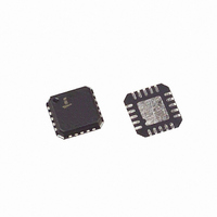
ISL6420IRZ Intersil, ISL6420IRZ Datasheet - Page 13

ISL6420IRZ
Manufacturer Part Number
ISL6420IRZ
Description
IC CTRLR PWM BUCK SYNC SGL 20QFN
Manufacturer
Intersil
Datasheet
1.ISL6420IRZ.pdf
(19 pages)
Specifications of ISL6420IRZ
Pwm Type
Voltage Mode
Number Of Outputs
1
Frequency - Max
1.4MHz
Duty Cycle
100%
Voltage - Supply
4.5 V ~ 16 V
Buck
Yes
Boost
No
Flyback
No
Inverting
No
Doubler
No
Divider
No
Cuk
No
Isolated
No
Operating Temperature
-40°C ~ 85°C
Package / Case
20-VQFN Exposed Pad, 20-HVQFN, 20-SQFN, 20-DHVQFN
Frequency-max
1.4MHz
Peak Reflow Compatible (260 C)
Yes
Rohs Compliant
Yes
Lead Free Status / RoHS Status
Lead free / RoHS Compliant
Available stocks
Company
Part Number
Manufacturer
Quantity
Price
Company:
Part Number:
ISL6420IRZ
Manufacturer:
Intersil
Quantity:
135
Company:
Part Number:
ISL6420IRZ
Manufacturer:
Intersil
Quantity:
150
Company:
Part Number:
ISL6420IRZ-TK
Manufacturer:
INTERSIL
Quantity:
4 823
A small ceramic capacitor should be placed in parallel with
R
presence of switching noise on the input voltage.
Voltage Margining
The ISL6420 has a voltage margining mode that can be
used for system testing. The voltage margining percentage
is resistor selectable up to ±10%. The voltage margining
mode can be enabled by connecting a margining set resistor
from VMSET/MODE pin to ground and using the control pins
GPIO1/REFIN and GPIO2 to toggle between positive and
negative margining (Refer to Table 2). With voltage
margining enabled, the VMSET resistor to ground sets a
current, which is switched to the FB pin. The current will be
equal to 2.468V divided by the value of the external resistor
tied to the VMSET/MODE pin.
The power supply output increases when GPIO2 is HIGH
and decreases when GPIO1/REFIN is HIGH. The amount
that the output voltage of the power supply changes with
voltage margining, will be equal to 2.468V times the ratio of
the external feedback resistor and the external resistor tied
to VMSET/MODE pin. Figure 9 shows the positive and
negative margining for a 3.3V output, using a 20.5kΩ
feedback resistor and using various VMSET resistor values.
I
Δ
VM
OCSET
V
FIGURE 10. VOLTAGE MARGINING vs VMSET RESISTANCE
VM
3.7
3.6
3.5
3.4
3.3
3.2
3.1
3.0
2.9
2.8
=
150
=
----------------------- -
R
2.468V
VMSET
2.468V
to smooth the voltage across R
175
----------------------- -
R
200
VMSET
R
FB
225
250
RVMSET (kΩ)
13
275
300
OCSET
325
350
in the
375
(EQ. 2)
(EQ. 3)
400
ISL6420
The slew time of the current is set by an external capacitor
on the CDEL pin, which is charged and discharged with a
100μA current source. The change in voltage on the
capacitor is 2.5V. This same capacitor is used to set the
PGOOD active delay after soft-start. When PGOOD is low,
the internal PGOOD circuitry uses the capacitor and when
PGOOD is high the voltage margining circuit uses the
capacitor. The slew time for voltage margining can be in the
range of 300µs to 2ms.
External Reference/DDR Supply
The voltage margining can be disabled by connecting the
VMSET/MODE to VCC5. In this mode the chip can be
configured to work with an external reference input and
provide a buffered reference output.
If VMSET/MODE pin and the GPIO1/REFIN pin are both tied
to VCC5, then the internal 0.6V reference is used as the
error amplifier non-inverting input. The buffered reference
output on REFOUT will be 0.6V ±0.01V, capable of sourcing
20mA and sinking up to 50µA current with a 2.2µF capacitor
connected to the REFOUT pin.
If VMSET/MODE pin is tied to high but GPIO1/REFIN is
connected to external voltage source between 0.6V to 1.25V,
then this external voltage is used as the reference voltage at
the positive input of the error amplifier. The buffered
reference output on REFOUT will be Vrefin ±0.01V, capable
of sourcing 20mA and sinking up to 50µA current with a
2.2µF capacitor on the REFOUT pin.
Power Good
The PGOOD pin can be used to monitor the status of the
output voltage. PGOOD will be true (open drain) when the
FB pin is within ±10% of the reference and the ENSS pin has
completed its soft-start ramp.
Additionally, a capacitor on the CDEL pin will set a delay for
the PGOOD signal. After the ENSS pin completes its soft-
start ramp, a 2µA current begins charging the CDEL
V
100m/DIV
FIGURE 11. VOLTAGE MARGINING SLEW TIME
V
100mV/DIV
OUT
OUT
2ms/DIV
February 13, 2008
FN9151.5


