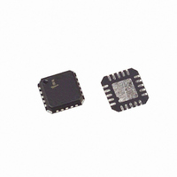
ISL6420IRZ Intersil, ISL6420IRZ Datasheet - Page 15

ISL6420IRZ
Manufacturer Part Number
ISL6420IRZ
Description
IC CTRLR PWM BUCK SYNC SGL 20QFN
Manufacturer
Intersil
Datasheet
1.ISL6420IRZ.pdf
(19 pages)
Specifications of ISL6420IRZ
Pwm Type
Voltage Mode
Number Of Outputs
1
Frequency - Max
1.4MHz
Duty Cycle
100%
Voltage - Supply
4.5 V ~ 16 V
Buck
Yes
Boost
No
Flyback
No
Inverting
No
Doubler
No
Divider
No
Cuk
No
Isolated
No
Operating Temperature
-40°C ~ 85°C
Package / Case
20-VQFN Exposed Pad, 20-HVQFN, 20-SQFN, 20-DHVQFN
Frequency-max
1.4MHz
Peak Reflow Compatible (260 C)
Yes
Rohs Compliant
Yes
Lead Free Status / RoHS Status
Lead free / RoHS Compliant
Available stocks
Company
Part Number
Manufacturer
Quantity
Price
Company:
Part Number:
ISL6420IRZ
Manufacturer:
Intersil
Quantity:
135
Company:
Part Number:
ISL6420IRZ
Manufacturer:
Intersil
Quantity:
150
Company:
Part Number:
ISL6420IRZ-TK
Manufacturer:
INTERSIL
Quantity:
4 823
oscillator (OSC) triangular wave to provide a pulse-width
modulated (PWM) wave with an amplitude of V
PHASE node. The PWM wave is smoothed by the output filter
(L
The modulator transfer function is the small-signal transfer
function of Vout/V
Gain and the output filter (L
break frequency at F
ENSS
FIGURE 14. PRINTED CIRCUIT BOARD SMALL SIGNAL
FIGURE 15. VOLTAGE - MODE BUCK CONVERTER
O
ΔV
C
SS
and C
OSC
OSC
ISL6420
O
GND
).
COMPARATOR
LAYOUT GUIDELINES
COMPENSATION DESIGN
ERROR
AMP
V
ISL6420
E/A
DETAILED COMPENSATION COMPONENTS
PWM
E/A
Z
+
-
COMP
+
FB
-
C1
LC
. This function is dominated by a DC
C
PHASE
VCC
BOOT
BOOT
REFERENCE
and a zero at F
C2
+5V
+
-
O
R2
DRIVER
DRIVER
15
C
Z
REF
and C
IN
VCC
D1
Z
FB
FB
O
V
), with a double pole
IN
PHASE
ESR
Q1
C3
(PARASITIC)
+V
Q2
Z
IN
. The DC Gain of
L
IN
O
R1
L
O
R3
IN
ESR
C
O
C
V
at the
O
OUT
V
OUT
V
OUT
ISL6420
the modulator is simply the input voltage (V
peak-to-peak oscillator voltage ΔV
Modulator Break Frequency Equations
The compensation network consists of the error amplifier
(internal to the ISL6420) and the impedance networks Z
and Z
a closed loop transfer function with the highest 0dB crossing
frequency (f
is the difference between the closed loop phase at f
180
network’s poles, zeros and gain to the components (R1, R2,
R3, C1, C2, and C3) in Figure 14. Use these guidelines for
locating the poles and zeros of the compensation network:
Compensation Break Frequency Equations
Figure 15 shows an asymptotic plot of the DC/DC
converter’s gain vs. frequency. The actual Modulator Gain
has a high gain peak do to the high Q factor of the output
filter and is not shown in Figure 15. Using the above
guidelines should give a Compensation Gain similar to the
curve plotted. The open loop error amplifier gain bounds the
compensation gain. Check the compensation gain at F
with the capabilities of the error amplifier. The Loop Gain is
constructed on the log-log graph of Figure 15 by adding the
Modulator Gain (in dB) to the Compensation Gain (in dB).
This is equivalent to multiplying the modulator transfer
F
F
F
F
F
F
1. Pick Gain (R2/R1) for desired converter bandwidth
2. Place 1
3. Place 2
4. Place 1
5. Place 2
6. Check Gain against Error Amplifier’s Open-Loop Gain
7. Estimate Phase Margin - Repeat if Necessary
LC
ESR
Z1
P1
Z2
P2
o
(~75% F
=
=
. The equations below relate the compensation
=
=
=
FB
=
-------------------------------------- -
2π
----------------------------------
2π R3 C3
----------------------------------
2π R
----------------------------------------------------- -
2π
------------------------------------------------------ -
2π R2
-------------------------------------------- -
2π
. The goal of the compensation network is to provide
•
•
•
•
•
•
(
ST
ND
ST
ND
0dB
1
L
(
R1
1
1
LC
ESR C
2 C1
O
•
•
Zero Below Filter’s Double Pole
Pole at the ESR Zero
•
1
Zero at Filter’s Double Pole
Pole at Half the Switching Frequency
)
•
) and adequate phase margin. Phase margin
+
1
1
⎛
⎝
C
R3
C1 C2
--------------------- -
C1
•
O
) C3
+
•
O
•
C2
)
⎞
⎠
OSC
.
IN
) divided by the
February 13, 2008
0dB
(EQ. 4)
(EQ. 5)
(EQ. 6)
(EQ. 7)
(EQ. 8)
(EQ. 9)
FN9151.5
P2
IN
and


