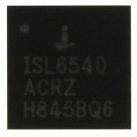
ISL8118IRZ Intersil, ISL8118IRZ Datasheet - Page 16

ISL8118IRZ
Manufacturer Part Number
ISL8118IRZ
Description
IC CTRLR PWM 1-PHASE 28-QFN
Manufacturer
Intersil
Datasheet
1.ISL8118CRZ.pdf
(20 pages)
Specifications of ISL8118IRZ
Pwm Type
Voltage Mode
Number Of Outputs
1
Frequency - Max
2MHz
Duty Cycle
100%
Voltage - Supply
2.97 V ~ 22 V
Buck
Yes
Boost
No
Flyback
No
Inverting
No
Doubler
No
Divider
No
Cuk
No
Isolated
No
Operating Temperature
-40°C ~ 85°C
Package / Case
28-VQFN Exposed Pad, 28-HVQFN, 28-SQFN, 28-DHVQFN
Frequency-max
2MHz
Rohs Compliant
YES
Lead Free Status / RoHS Status
Lead free / RoHS Compliant
Available stocks
Company
Part Number
Manufacturer
Quantity
Price
Company:
Part Number:
ISL8118IRZ
Manufacturer:
Intersil
Quantity:
120
Part Number:
ISL8118IRZ
Manufacturer:
INTERSIL
Quantity:
20 000
Figure 8 shows the circuit traces that require additional
layout consideration. Use single point and ground plane
construction for the circuits shown. Minimize any leakage
current paths on the SS pin and locate the capacitor, CSS
close to the SS pin (as described earlier) as the internal
current source is only 38µA. Provide local decoupling
between PVCC and PGND pins as described earlier. Locate
the capacitor, CBOOT as close as practical to the BOOT and
LX pins.
Compensating the Converter
The ISL8118 single-phase converter is a voltage-mode
controller. This section highlights the design considerations for
a voltage-mode controller requiring external compensation. To
address a broad range of applications, a type-3 feedback
network is recommended (see Figure 9).
Figure 10 highlights the voltage-mode control loop for a
synchronous-rectified buck converter, when using an internal
differential remote sense amplifier. The output voltage (V
is regulated to the reference voltage, VREF, level. The error
amplifier output (COMP pin voltage) is compared with the
oscillator (OSC) triangle wave to provide a pulse-width
modulated wave with an amplitude of V
PWM wave is smoothed by the output filter (L and C). The
output filter capacitor bank’s equivalent series resistance is
represented by the series resistor ESR.
The modulator transfer function is the small-signal transfer
function of V
gain, given by d
filter, with a double pole break frequency at F
F
the total output capacitance and its equivalent series
resistance.
F
F
CE
LC
CE
FIGURE 9. COMPENSATION CONFIGURATION FOR ISL8118
. For the purpose of this analysis C and ESR represent
=
=
---------------------------
2π
-------------------------------- -
2π C ESR
C
R
3
⋅
3
⋅
1
L C
OUT
1
⋅
WHEN USING DIFFERENTIAL REMOTE SENSE
⋅
MAX
/V
COMP
V
R
IN
R
1
2
/V
. This function is dominated by a DC
OSC
C
2
C
16
, and shaped by the output
1
COMP
VDIFF
FB
IN
at the LX node. The
LC
ISL8118
and a zero at
(EQ. 7)
(EQ. 8)
OUT
)
ISL8118
The compensation network consists of the error amplifier
(internal to the ISL8118) and the external R
components. The goal of the compensation network is to
provide a closed loop transfer function with high 0dB crossing
frequency (F
phase margin (better than 45°). Phase margin is the
difference between the closed loop phase at F
The equations that follow relate the compensation network’s
poles, zeros and gain to the components (R
and C
locating the poles and zeros of the compensation network:
1. Select a value for R
FIGURE 10. VOLTAGE-MODE BUCK CONVERTER
value for R
setting the output voltage to be equal to the reference set
voltage as shown in Figure 9, the design procedure can
be followed as presented. However, when setting the
output voltage via a resistor divider placed at the input of
the differential amplifier (as shown in Figure 10), in order
to compensate for the attenuation introduced by the
resistor divider, the below obtained R
multiplied by a factor of (R
remainder of the calculations remain unchanged, as long
as the compensated R
R
CIRCUIT
2
PWM
3
) in Figures 9 and 10. Use the following guidelines for
=
-------------------------------------------- -
d
V
COMP
MAX
OSC
0
COMPENSATION DESIGN
; typically 0.1 to 0.3 of F
2
HALF-BRIDGE
⋅
OSCILLATOR
V
for desired converter bandwidth (F
⋅
V
R
IN
OSC
E/A
DRIVE
1
⋅
⋅
R
F
ISL8118
F
2
LC
0
1
C
+
-
+
(1kΩ to 10kΩ, typically). Calculate
VREF
2
-
2
C
value is used.
1
OS
FB
BGATE
TGATE
VSENSN
VSENSP
VDIFF
EXTERNAL CIRCUIT
+ R
LX
SW
R
FB
3
V
IN
)/R
) and adequate
R
2
C
1
1
1
SEN
value needs be
OS
-R
, R
C
L
3
0dB
3
. The
2
, C
, R
DCR
R
and 180°.
1
V
3
ESR
OS
-C
OUT
0
, C
C
April 7, 2009
). If
R
3
(EQ. 9)
FB
FN6325.1
1
, C
2
,


