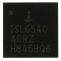
ISL8118IRZ Intersil, ISL8118IRZ Datasheet - Page 9

ISL8118IRZ
Manufacturer Part Number
ISL8118IRZ
Description
IC CTRLR PWM 1-PHASE 28-QFN
Manufacturer
Intersil
Datasheet
1.ISL8118CRZ.pdf
(20 pages)
Specifications of ISL8118IRZ
Pwm Type
Voltage Mode
Number Of Outputs
1
Frequency - Max
2MHz
Duty Cycle
100%
Voltage - Supply
2.97 V ~ 22 V
Buck
Yes
Boost
No
Flyback
No
Inverting
No
Doubler
No
Divider
No
Cuk
No
Isolated
No
Operating Temperature
-40°C ~ 85°C
Package / Case
28-VQFN Exposed Pad, 28-HVQFN, 28-SQFN, 28-DHVQFN
Frequency-max
2MHz
Rohs Compliant
YES
Lead Free Status / RoHS Status
Lead free / RoHS Compliant
Available stocks
Company
Part Number
Manufacturer
Quantity
Price
Company:
Part Number:
ISL8118IRZ
Manufacturer:
Intersil
Quantity:
120
Part Number:
ISL8118IRZ
Manufacturer:
INTERSIL
Quantity:
20 000
Electrical Specifications
NOTE:
Functional Pin Descriptions
VSENSP (Pin 1)
This pin provides differential remote sense for the ISL8118. It
is the positive input of a standard instrumentation amplifier
topology with unity gain, and should connect to the positive
rail of the load/processor. The voltage at this pin should be
set equal to the internal system reference voltage (0.591V
typical).
VSENSN (Pin 2)
This pin provides differential remote sense for the regulator.
It is the negative input of the instrumentation amplifier, and
should connect to the negative rail of the load/processor.
Typically 6µA is sourced from this pin. The output of the
remote sense buffer is disabled (High Impedance) by pulling
VSENSN to VCC.
REFOUT (Pin 3)
This pin connects to the unmargined system reference
through an internal buffer. It has a 19mA drive capability with
an output common mode range of GND to VCC. The
REFOUT buffer requires at least 1µF of capacitive loading to
be stable. This pin should not be left floating.
REFIN (Pin 4)
When the external reference pin (REFIN) is NOT within
~800mV of VCC, the REFIN pin is used as the system
reference instead of the internal 0.591V reference. The
recommended REFIN input voltage range is ~60mV to
VCC - 1.8V.
SS (Pin 5)
This pin provides soft-start functionality for the ISL8118. A
capacitor connected to ground along with the internal 38µA
Operational Transconductance Amplifier (OTA), sets the soft-
start interval of the converter. This pin is directly connected to
the non-inverting input of the Error Amplifier. To prevent noise
injection into the error amplifier, the SS capacitor should be
located within 150 mils of the SS and GND pins.
OFSP (Pin 6)
This pin sets the positive margining offset voltage. Resistors
should be connected to GND (R
from this pin. With MARGIN logic low, the internal 0.591V
Margining Transfer Ratio
Positive Margining Threshold
Negative Margining Threshold
Tri-state Input Level
3. Limits should be considered typical and are not production tested.
PARAMETER
9
Recommended Operating Conditions, Unless Otherwise Noted. Parameters with MIN and/or MAX limits are
100% tested at +25°C, unless otherwise specified. Temperature limits established by characterization and are
not production tested. (Continued)
OFSP
SYMBOL
MARGIN
MARGIN
MARGIN
N
) and OFSN (R
MARG
N
Disable Mode
MARG
MARG
= (V
)
ISL8118
TEST CONDITIONS
OFSN
-V
OFSP
reference is developed at the OFSP pin across resistor
R
R
OFSN is divided by 5 and imposed on the system reference.
The maximum designed offset of 1V between OFSP and
OFSN pins translates to a 200mV offset.
OFSN (Pin 7)
This pin sets the negative margining offset voltage. Resistors
should be connected to GND (R
from this pin. With MARGIN logic low, the internal 0.591V
reference is developed at the OFSN pin across resistor
R
R
OFSN is divided by 5 and imposed on the system reference.
The maximum designed offset of -1V between OFSP and
OFSN pins translates to a -200mV offset of the system
reference.
VCC (Pin 8, Analog Circuit Bias)
This pin provides power for the ISL8118 analog circuitry. The
pin should be connected to a 2.9V to 5.6V bias through an
RC filter from PVCC to prevent noise injection into the
analog circuitry. This pin can be powered off the internal or
external linear regulator options.
MARGIN (Pin 9)
The MARGIN pin controls margining function, a logic high
enables positive margining, a logic low sets negative
margining, a high impedance disables margining.
PGDLY (Pin 10)
Provides the ability to delay the output of the PGOOD
assertion by connecting a capacitor from this pin to GND. A
0.1µF capacitor produces approximately a 5ms delay.
PGOOD (Pin 11)
Provides an open drain Power Good signal when the output
is within 9% of nominal output regulation point with 6%
hysteresis (15%/9%), and after soft-start is complete.
PGOOD monitors the VDIFF pin.
EN (Pin 12)
This pin is compared with an internal 0.50V reference and
enables the soft-start cycle. This pin also can be used for
OFSP
MARG
OFSN
MARG
)/V
MARG
. The voltage on OFSP is driven from OFSN through
. The voltage on OFSN is driven from OFSP through
. The resulting voltage differential between OFSP and
. The resulting voltage differential between OFSP and
4.84
1.51
0.75
1.21
MIN
OFSN
1.325
TYP
1.8
0.9
5
) and OFSP (R
MAX
5.22
2.02
1.05
1.40
MARG
April 7, 2009
FN6325.1
UNITS
SDR
V
V
V
)


