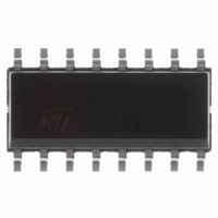
L6910TR STMicroelectronics, L6910TR Datasheet - Page 7

L6910TR
Manufacturer Part Number
L6910TR
Description
IC PWM BUCK BST VM 16SOIC
Manufacturer
STMicroelectronics
Datasheet
1.L6910ATR.pdf
(29 pages)
Specifications of L6910TR
Pwm Type
Voltage Mode
Number Of Outputs
1
Frequency - Max
230kHz
Duty Cycle
100%
Voltage - Supply
5 V ~ 12 V
Buck
Yes
Boost
Yes
Flyback
No
Inverting
No
Doubler
No
Divider
No
Cuk
No
Isolated
No
Operating Temperature
-40°C ~ 150°C
Package / Case
16-SOIC (3.9mm Width)
Frequency-max
230kHz
Operating Temperature Range
- 40 C to + 150 C
Mounting Style
SMD/SMT
Lead Free Status / RoHS Status
Lead free / RoHS Compliant
Other names
497-3656
497-3656-2
497-3656
497-3656-2
497-3656
Available stocks
Company
Part Number
Manufacturer
Quantity
Price
Part Number:
L6910TR
Manufacturer:
ST
Quantity:
20 000
L6910 - L6910A
avoided if the PHASE pin is over about 500mV. The lower mos is in any case turned-on after 200ns from the
high side turn-off.
The peak current is shown for both the upper (fig. 6) and the lower (fig. 7) driver at 5V and 12V. A 3.3nF capac-
itive load has been used in these measurements.
For the lower driver, the source peak current is 1.1A @ V
= 12V and 500mA @ V
= 5V, and the sink peak
CC
CC
current is 1.3A @ V
= 12V and 500mA @ V
= 5V.
CC
CC
Similarly, for the upper driver, the source peak current is 1.3A @ Vboot-Vphase = 12V and 600mA @ Vboot-
Vphase = 5V, and the sink peak current is 1.3A @ Vboot-Vphase =12V and 550mA @ Vboot-Vphase = 5V.
Figure 6. High Side Driver Peak Current. Vboot-Vphase = 12V (right) Vboot-Vphase = 5V (left)
CH1 = High Side Gate CH4 = Gate Current
Figure 7. Low Side Driver Peak Current. V
= 12V (right) V
= 5V (left)
CC
CC
CH1 = Low Side Gate CH4 = Gate Current
4.5 Monitoring and Protections
The output voltage is monitored by means of pin FB. If it is not within ±10% (typ.) of the programmed value, the
powergood output is forced low.
The device provides overvoltage protection, when the voltage sensed on pin FB reaches a value 17% (typ.)
greater than the reference the OSC pin is forced high (3V typ.) and the lower driver is turned on as long as the
over-voltage is detected.
7/29


