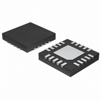
ISL62872HRUZ-T Intersil, ISL62872HRUZ-T Datasheet - Page 18

ISL62872HRUZ-T
Manufacturer Part Number
ISL62872HRUZ-T
Description
IC CTRLR DC/DC PWM 20-TQFN
Manufacturer
Intersil
Datasheet
1.ISL62871HRUZ-T.pdf
(25 pages)
Specifications of ISL62872HRUZ-T
Pwm Type
Controller
Number Of Outputs
1
Frequency - Max
330kHz
Duty Cycle
100%
Voltage - Supply
3.3 V ~ 25 V
Buck
Yes
Boost
No
Flyback
No
Inverting
No
Doubler
No
Divider
No
Cuk
No
Isolated
No
Operating Temperature
-10°C ~ 100°C
Package / Case
16-UTQFN (16-µTQFN)
Frequency-max
330kHz
Lead Free Status / RoHS Status
Lead free / RoHS Compliant
Available stocks
Company
Part Number
Manufacturer
Quantity
Price
Part Number:
ISL62872HRUZ-T
Manufacturer:
INTERSIL
Quantity:
20 000
destruction of circuit components, as well as nuisance OCP
faults.
A DC/DC buck regulator must have output capacitance C
into which ripple current I
a corresponding ripple voltage V
sum of the voltage drop across the capacitor ESR and of the
voltage change stemming from charge moved in and out of
the capacitor. These two voltages are expressed in
Equations 33 and 34:
ΔΔV
If the output of the converter has to support a load with high
pulsating current, several capacitors will need to be paralleled
to reduce the total ESR until the required V
The inductance of the capacitor can cause a brief voltage dip
if the load transient has an extremely high slew rate. Low
inductance capacitors should be considered. A capacitor
dissipates heat as a function of RMS current and frequency.
Be sure that I
capacitors so that they operate below the maximum rated
RMS current at F
a capacitor can fade as much as 50% as the DC voltage
across it increases.
Selection of the Input Capacitor
The important parameters for the bulk input capacitance are
the voltage rating and the RMS current rating. For reliable
operation, select bulk capacitors with voltage and current
ratings above the maximum input voltage and capable of
supplying the RMS current required by the switching circuit.
Their voltage rating should be at least 1.25x greater than the
maximum input voltage, while a voltage rating of 1.5x is a
preferred rating. Figure 14 is a graph of the input RMS ripple
current, normalized relative to output load current, as a
function of duty cycle that is adjusted for converter efficiency.
The ripple current calculation is written as Equation 35:
Where:
Duty cycle is written as Equation 36:
ΔV
I
D
IN_RMS
- I
- x is a multiplier (0 to 1) corresponding to the inductor
- D is the duty cycle that is adjusted to take into account
=
ESR
C
peak-to-peak ripple amplitude expressed as a
percentage of I
the efficiency of the converter
------------------------- -
V
MAX
IN
=
=
V
-------------------------------- -
8 C
⋅
=
O
EFF
I
⋅
is the maximum continuous I
P-P
---------------------------------------------------------------------------------------------------- -
I
O
P-P
(
P-P
I
⋅ SR
MAX
⋅
E
F
is shared by a sufficient quantity of paralleled
SW
SW
2
MAX
. Take into account that the rated value of
⋅
(
D D
–
(0% to 100%)
P-P
I
2
MAX
)
)
18
can flow. Current I
+
⎛
⎝
P-P
x I
⋅
MAX
across C
LOAD
2
⋅
----- -
12
P-P
D
⎞
⎠
of the converter
O,
is achieved.
P-P
which is the
develops
ISL62871, ISL62872
(EQ. 33)
(EQ. 34)
(EQ. 35)
(EQ. 36)
O
In addition to the bulk capacitance, some low ESL ceramic
capacitance is recommended to decouple between the drain
of the high-side MOSFET and the source of the low-side
MOSFET.
Selecting The Bootstrap Capacitor
Adding an external capacitor across the BOOT and PHASE
pins completes the bootstrap circuit. We selected the
bootstrap capacitor breakdown voltage to be at least 10V.
Although the theoretical maximum voltage of the capacitor is
PVCC-V
excursions below ground by the phase node requires we
select a capacitor with at least a breakdown rating of 10V. The
bootstrap capacitor can be chosen from Equation 37:
Where:
As an example, suppose an upper MOSFET has a gate
charge, Q
the drive voltage over a PWM cycle is 200mV. One will find that
a bootstrap capacitance of at least 0.125µF is required. The
next larger standard value capacitance is 0.15µF. A good
quality ceramic capacitor such as X7R or X5R is
recommended.
C
FIGURE 14. NORMALIZED RMS INPUT CURRENT FOR x = 0.8
BOOT
- Q
- ΔV
charge the gate of the upper MOSFET
capacitor
0.60
0.55
0.50
0.45
0.40
0.35
0.30
0.25
0.20
0.15
0.10
0.05
GATE
BOOT
≥
0
DIODE
0
----------------------- -
ΔV
GATE
Q
GATE
BOOT
is the amount of gate charge required to fully
0.1
is the maximum decay across the BOOT
, of 25nC at 5V and also assume the droop in
(voltage drop across the boot diode), large
0.2
0.3
0.4
DUTY CYCLE
x = 0.25
0.5
0.6
x = 0
x = 1
0.7
x = 0.75
0.8
August 14, 2008
x = 0.50
0.9
(EQ. 37)
FN6707.0
1.0


