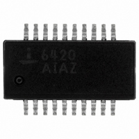
ISL6420AIAZ-TK Intersil, ISL6420AIAZ-TK Datasheet - Page 15

ISL6420AIAZ-TK
Manufacturer Part Number
ISL6420AIAZ-TK
Description
IC CTRLR PWM SYNC BUCK 20-QSOP
Manufacturer
Intersil
Specifications of ISL6420AIAZ-TK
Pwm Type
Voltage Mode
Number Of Outputs
1
Frequency - Max
1.4MHz
Duty Cycle
100%
Voltage - Supply
4.5 V ~ 28 V
Buck
Yes
Boost
No
Flyback
No
Inverting
No
Doubler
No
Divider
No
Cuk
No
Isolated
No
Operating Temperature
-40°C ~ 85°C
Package / Case
20-QSOP
Frequency-max
1.4MHz
Lead Free Status / RoHS Status
Lead free / RoHS Compliant
Other names
ISL6420AIAZ-TKTR
Available stocks
Company
Part Number
Manufacturer
Quantity
Price
Company:
Part Number:
ISL6420AIAZ-TK
Manufacturer:
Intersil
Quantity:
2 400
Figure 14 shows the critical power components of the
converter. To minimize the voltage overshoot the
interconnecting wires indicated by heavy lines should be part
of ground or power plane in a printed circuit board. The
components shown in Figure 14 should be located as close
together as possible. Please note that the capacitors C
and C
Locate the ISL6420A within 3 inches of the MOSFETs, Q1
and Q2. The circuit traces for the MOSFETs’ gate and
source connections from the ISL6420A must be sized to
handle up to 2A peak current.
Figure 15 shows the circuit traces that require additional
layout consideration. Use single point and ground plane
construction for the circuits shown. Minimize any leakage
current paths on the SS PIN and locate the capacitor, C
close to the SS pin because the internal current source is
only 30µA. Provide local V
GND pins. Locate the capacitor, C
to the BOOT and PHASE pins.
SS/EN
FIGURE 15. PRINTED CIRCUIT BOARD SMALL SIGNAL
C
SS
O
each represent numerous physical capacitors.
ISL6420A
GND
LAYOUT GUIDELINES
PHASE
C
VCC
BOOT
BOOT
+5V
CC
15
decoupling between VCC and
C
VCC
D1
BOOT
as close as practical
Q1
+V
Q2
IN
L
O
C
O
IN
V
ss
OUT
ISL6420A
Feedback Compensation
Figure 16 highlights the voltage-mode control loop for a
synchronous-rectified buck converter. The output voltage
(Vout) is regulated to the Reference voltage level. The error
amplifier (Error Amp) output (V
oscillator (OSC) triangular wave to provide a pulse-width
modulated (PWM) wave with an amplitude of V
PHASE node. The PWM wave is smoothed by the output filter
(L
The modulator transfer function is the small-signal transfer
function of Vout/V
Gain and the output filter (L
break frequency at F
the modulator is simply the input voltage (V
peak-to-peak oscillator voltage DV
FIGURE 16. VOLTAGE - MODE BUCK CONVERTER
O
∆V
and C
OSC
OSC
O
).
COMPARATOR
COMPENSATION DESIGN
ERROR
AMP
V
ISL6420A
E/A
DETAILED COMPENSATION COMPONENTS
PWM
E/A
Z
+
-
COMP
FB
+
-
LC
C1
. This function is dominated by a DC
REFERENCE
and a zero at F
C2
+
-
O
R2
DRIVER
DRIVER
REF
Z
and C
IN
E/A
Z
) is compared with the
OSC
FB
FB
O
V
), with a double pole
IN
.
PHASE
ESR
C3
(PARASITIC)
IN
Z
. The DC Gain of
L
IN
R1
O
) divided by the
R3
IN
ESR
C
October 13, 2005
V
at the
O
OUT
V
FN9169.1
OUT


