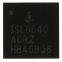
ISL6540AIRZ-T Intersil, ISL6540AIRZ-T Datasheet - Page 10

ISL6540AIRZ-T
Manufacturer Part Number
ISL6540AIRZ-T
Description
IC CTRLR PWM BUCK 1PHASE 28-QFN
Manufacturer
Intersil
Datasheet
1.ISL6540ACRZ-T.pdf
(22 pages)
Specifications of ISL6540AIRZ-T
Pwm Type
Voltage Mode
Number Of Outputs
1
Frequency - Max
2MHz
Duty Cycle
100%
Voltage - Supply
2.97 V ~ 22 V
Buck
Yes
Boost
No
Flyback
No
Inverting
No
Doubler
No
Divider
No
Cuk
No
Isolated
No
Operating Temperature
-40°C ~ 85°C
Package / Case
28-VQFN Exposed Pad, 28-HVQFN, 28-SQFN, 28-DHVQFN
Frequency-max
2MHz
Lead Free Status / RoHS Status
Lead free / RoHS Compliant
transient voltages that could result in electrical overstress
(EOS) damage. It is recommended that a 1kΩ resistor be
placed in series with this pin.
VFF (Pin 13)
The voltage at this pin is used for input voltage feed-forward
compensation and sets the internal oscillator ramp
peak-to-peak amplitude at 0.16*VFF. An external RC filter
may be required at this pin in noisy input environments. The
minimum recommended VFF voltage is 2.97V.
VIN (Pin 14, Internal Linear Regulator Input)
This pin should be tied directly to the input rail when using
the internal or external linear regulator options. It provides
power to the External/Internal linear drive circuitry. When
used with an external 3.3V to 5V supply, this pin should be
tied directly to PVCC.
LIN_DRV (Pin 15, External Linear Regulator Drive)
This pin allows the use of an external pass element to power
the IC for input voltages above 5.0V. It should be connected
to GND when using an external 5V supply or the internal
linear regulator. When using the external linear regulator
option, this pin should be connected to the gate of a PMOS
pass element, a pull-up resistor must be connected between
the PMOS device’s gate and source for proper operation.
PVCC (Pin 16, Driver Bias Voltage)
This pin is the output of the internal series linear regulator. It
also provides the bias for both low side and high side
MOSFET drivers. The maximum voltage differential between
PVCC and PGND is 6V. Its recommended operational
voltage range is 2.9V to 5.5V. At minimum, a 10µF capacitor
is required for decoupling PVCC to PGND. For proper
operation the PVCC capacitor should be located next to the
PVCC and the PGND pins and should be connected to these
pins with dedicated traces.
LGATE (Pin 17)
This pin provides the drive for the low side MOSFET and
should be connected to its gate.
PGND (Pin 18, Power Ground)
This pin connects to the low side MOSFET's source and
provides the ground return path for the lower MOSFET driver
and internal power circuitries. In addition, PGND is the return
path for the low side MOSFET’s r
circuit.
PHASE (Pin 19)
This pin connects to the source of the high side MOSFET
and the drain of the low side MOSFET. This pin represents
the return path for the high side gate driver. During normal
switching, this pin is used for high side and low side current
sensing.
10
DS(ON)
current sensing
ISL6540A
UGATE (Pin 20)
This pin provides the drive for the high side MOSFET and
should be connected to its gate.
BOOT (Pin 21)
This pin provides the bootstrap bias for the high side driver.
The absolute maximum voltage differential between BOOT
and PHASE is 6.0V (including the voltage added due to the
overcharging of the bootstrap capacitor); its operational
voltage range is 2.5V to 5.5V with respect to PHASE. Should
overcharging of the BOOT capacitor occur, it is
recommended that a 2.2Ω resistor be placed in series with
the bootstrap diode.
HSOC (Pin 22)
The high side sourcing current limit is set by connecting this
pin with a resistor and capacitor to the drain of the high side
MOSFET. A 100µA current source develops a voltage
across the resistor which is then compared with the voltage
developed across the high side MOSFET. An initial ~120ns
blanking period is used to eliminate sampling error due to
the switching noise before the current is measured.
LSOC (Pin 23)
The low side source and sinking current limit is set by
placing a resistor (R
and PGND. A 100µA current source develops a voltage
across R
developed across the low side MOSFET when on. The
sinking current limit is set at 1x of the nominal sourcing limit
in ISL6540A. An initial ~120ns blanking period is used to
eliminate the sampling error due to switching noise before
the current is measured.
FS (Pin 24)
This pin provides oscillator switching frequency adjustment
by placing a resistor (R
COMP (Pin 25)
This pin is the error amplifier output. It should be connected
to the FB pin through the desired compensation network.
FB (Pin 26)
This pin is the inverting input of the error amplifier and has a
maximum usable voltage of VCC - 1.8V. When using the
internal differential remote sense functionality, this pin
should be connected to VMON by a standard feedback
network. In the event the remote sense buffer is disabled,
the VMON pin should be connected to VOUT by a resistor
divider along with FB’s compensation network.
GND (Pin 27, Analog Ground)
Signal ground for the IC. All voltage levels are measured
with respect to this pin. This pin should not be left floating.
VMON (Pin 28)
This pin is the output of the differential remote sense
instrumentation amplifier. It is connected internally to the
LSOC
which is then compared with the voltage
LSOC
FS
) and capacitor between this pin
) from this pin to GND.
October 7, 2008
FN6288.5


