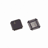
ISL6420IR Intersil, ISL6420IR Datasheet

ISL6420IR
Specifications of ISL6420IR
Available stocks
Related parts for ISL6420IR
ISL6420IR Summary of contents
Page 1
... CAUTION: These devices are sensitive to electrostatic discharge; follow proper IC Handling Procedures. | 1-888-INTERSIL or 1-888-468-3774 Intersil (and design registered trademark of Intersil Americas Inc. Copyright © Intersil Americas Inc. 2004-2005, 2008. All Rights Reserved All other trademarks mentioned are the property of their respective owners. ...
Page 2
... Ordering Information PART NUMBER PART MARKING ISL6420IR ISL 6420IRZ ISL6420IR-T* ISL 6420IRZ ISL6420IRZ (Note) 64 20IRZ ISL6420IRZ-T* (Note) 64 20IRZ ISL6420IRZ-TK* (Note) 64 20IRZ ISL6420IA ISL 6420IA ISL6420IA-TK* ISL 6420IA ISL6420IAZ (Note) ISL 6420IAZ ISL6420IAZ-TK* (Note) ISL 6420IAZ *Please refer to TB347 for details on reel specifications. ...
Page 3
Functional Block Diagram SGND SS FB COMP GPIO1/REFIN GPIO2 REFOUT VOLTAGE MARGINING VMSET/MODE Typical 5V Input DC/DC Application Schematic VIN ENSS RT PGOOD C7 R2 0.1µF CDEL C8 SGND ISL6420 VIN VCC5 OCSET ...
Page 4
Typical 12V Input DC/DC Application Schematic 12V C1 C2 ENSS RT PGOOD R2 C7 CDEL C8 SGND Typical 5V Input DC/DC Application Schematic VIN SS/EN RT CDEL R2 C7 PGOOD REF SGND FB R3 ...
Page 5
Typical 12V Input DC/DC Application Schematic 12V C1 C2 VIN SS/EN RT CDEL R2 C7 PGOOD SGND CONFIGURATION FOR DDR TERMINATION/EXTERNALLY REFERENCED TRACKING APPLICATIONS 5 ISL6420 C3 C4 PVCC VCC5 OCSET MONITOR AND PROTECTION BOOT UGATE OSC ...
Page 6
... Maximum Junction Temperature (Plastic Package +150°C Maximum Storage Temperature Range . . . . . . . . . .-65°C to +150°C Ambient Temperature Range -40°C to +85°C (for “I” suffix) Junction Temperature Range .-40°C to +125°C Pb-free reflow profile . . . . . . . . . . . . . . . . . . . . . . . . . .see link below http://www.intersil.com/pbfree/Pb-FreeReflow.asp SYMBOL TEST CONDITIONS ENSS = GND VIN = VCC5 for 5V configuration VIN = 5 ...
Page 7
Electrical Specifications Operating Conditions, Unless Otherwise Noted: VIN = 12V, PV PARAMETER REFERENCE AND SOFT-START/ENABLE Internal Reference Voltage Soft-Start Current Soft-Start Threshold Enable Low (Converter disabled) PWM CONTROLLER GATE DRIVERS Gate Drive Peak Current Rise Time Fall Time Dead Time ...
Page 8
Electrical Specifications Operating Conditions, Unless Otherwise Noted: VIN = 12V, PV PARAMETER ISET1 on FB Pin ISET2 on FB Pin THERMAL SHUTDOWN Shutdown Temperature (Note 7) Thermal Shutdown Hysteresis (Note 7) NOTES: 4. The operating supply current and shutdown current ...
Page 9
Typical Performance Curves 0.604 0.602 0.6 0.598 0.596 0.594 -40 -15 10 TEMPERATURE (°C) FIGURE 1. VREF vs. TEMPERATURE 1.15 1.05 0.95 0.85 -40 -15 10 TEMPERATURE (°C) FIGURE 3. IOCSET vs. TEMPERATURE FIGURE 5. PWM WAVEFORMS 9 ISL6420 320 ...
Page 10
Pin Descriptions VIN This pin powers the controller and must be closely decoupled to ground using a ceramic capacitor as close to the VIN pin as possible. TABLE 1. INPUT SUPPLY CONFIGURATION INPUT PIN CONFIGURATION 5.6V to 16V Connect the ...
Page 11
GPIO1/REFIN This is a dual function pin. If VMSET/MODE is not connected to VCC5 then this pin serves as GPIO1. Refer to Table 2 for GPIO1 commands interpretation. If VMSET/MODE is connected to VCC5 then this pin will serve as ...
Page 12
Functional Description Initialization The ISL6420 automatically initializes upon receipt of power. The Power-On Reset (POR) function monitors the internal bias voltage generated from LDO output (VCC5) and the ENSS pin. The POR function initiates the soft-start operation after the VCC5 ...
Page 13
A small ceramic capacitor should be placed in parallel with R to smooth the voltage across R OCSET presence of switching noise on the input voltage. Voltage Margining The ISL6420 has a voltage margining mode that can be used for ...
Page 14
The capacitor will be quickly discharged before PGOOD goes high. The programmable delay can be used to sequence multiple converters LOW-true reset signal. FIGURE 12. PGOOD DELAY If the voltage on the FB pin ...
Page 15
BOOT D1 C BOOT ISL6420 PHASE ENSS +5V VCC C VCC C SS GND FIGURE 14. PRINTED CIRCUIT BOARD SMALL SIGNAL LAYOUT GUIDELINES V OSC DRIVER PWM COMPARATOR - DRIVER ΔV + OSC E ...
Page 16
20LOG (R2/R1) 20 20LOG Δ MODULATOR -20 GAIN - ESR -60 ...
Page 17
Be sure to check both of these equations at the minimum and maximum output levels for the worst case response time. Input Capacitor Selection Use a mix of input bypass capacitors to control the voltage overshoot across ...
Page 18
Package Outline Drawing L20.4x4 20 LEAD QUAD FLAT NO-LEAD PLASTIC PACKAGE Rev 1, 11/06 4.00 6 PIN 1 INDEX AREA 0.15 (4X) TOP VIEW ( 3. 6 TYP ) ( TYPICAL RECOMMENDED LAND PATTERN 18 ISL6420 16X ...
Page 19
... Accordingly, the reader is cautioned to verify that data sheets are current before placing orders. Information furnished by Intersil is believed to be accurate and reliable. However, no responsibility is assumed by Intersil or its subsidiaries for its use; nor for any infringements of patents or other rights of third parties which may result from its use ...


