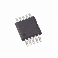
EL7512CYZ-T7 Intersil, EL7512CYZ-T7 Datasheet - Page 2

EL7512CYZ-T7
Manufacturer Part Number
EL7512CYZ-T7
Description
IC REG PWM STEP-UP 10-MSOP
Manufacturer
Intersil
Datasheet
1.EL7512CY.pdf
(8 pages)
Specifications of EL7512CYZ-T7
Pwm Type
Controller
Number Of Outputs
1
Frequency - Max
1.2MHz
Duty Cycle
90%
Voltage - Supply
2 V ~ 12 V
Buck
No
Boost
Yes
Flyback
No
Inverting
No
Doubler
No
Divider
No
Cuk
No
Isolated
No
Operating Temperature
-40°C ~ 85°C
Package / Case
10-MSOP, Micro10™, 10-uMAX, 10-uSOP
Frequency-max
1.2MHz
Lead Free Status / RoHS Status
Lead free / RoHS Compliant
Electrical Specifications
Absolute Maximum Ratings
EN, LBI, . . . . . . . . . . . . . . . . . . . . . . . . . . . . . . . . . . . . . . . . . . .+18V
LX . . . . . . . . . . . . . . . . . . . . . . . . . . . . . . . . . . . . . . . . . . . . . . . .20V
V
CAUTION: Stresses above those listed in “Absolute Maximum Ratings” may cause permanent damage to the device. This is a stress only rating and operation of the
device at these or any other conditions above those indicated in the operational sections of this specification is not implied.
IMPORTANT NOTE: All parameters having Min/Max specifications are guaranteed. Typical values are for information purposes only. Unless otherwise noted, all tests
are at the specified temperature and are pulsed tests, therefore: T
Pin Descriptions
IQ1
IQ2
VFB
IB
V
D
I
I
V
V
I
R
I
∆V
∆V
F
F
VHI_EN
VLO_EN
LIM
SHDN
LEAK-LBO
LEAK-SWITCH
DD
PARAMETER
PIN NUMBER
IN
LBI
OL-LBO
OSC-MAX
OSC1
MAX
DS-ON
OUT
OUT
. . . . . . . . . . . . . . . . . . . . . . . . . . . . . . . . . . . . . . . . . . . . . . .12V
/∆V
/∆I
10
1
2
3
4
5
6
7
8
9
OUT
IN
Quiescent Current - Shut-down
Quiensent Current
Feedback Voltage
Feedback Input Bias Current
Input Voltage Range
Maximum Duty Cycle
Current Limit - Max Average Input
Current
Shut-down Input Bias Current
LBI Threshold Voltage
LBO Output Low
LBO Output Leakage Current
Switch On Resistance
Switch Leakage Current
Line Regulation
Load Regulation
Maximum Switching Frequency
Switching Frequency
EN Input High Threshold
EN Input Low Threshold
PIN NAME
PGND
SGND
LBO
VDD
EN
LBI
RT
SS
FB
LX
DESCRIPTION
2
V
Power ground; connected to the source of internal N-channel power MOSFET
Signal ground; ground reference for all the control circuitry; needs to have only a single connection to PGND
Timing resistor to adjust the oscillation frequency of the converter
Chip enable; connects to logic HI (>1.6V) for chip to function
Low battery input; connects to a sensing voltage, or left open if function is not used
Low battery detection output; connected to the open drain of a MOSFET; able to sink 1mA current
Soft-start; connects to a capacitor to control the start-up of the converter
Voltage feedback input; needs to connect to resistor divider to decide V
Control circuit positive supply
Inductor drive pin; connected to the drain of internal N-channel power MOSFET
IN
(T
= 5V, V
A
= 25°C)
OUT
= 12V, I
J
= T
OUT
VEN = 2V
ILBO = 1mA
VLBI = 250mV, VLBO = 5V
3V < V
I
R
VEN = 0
at 12V output
C
OUT
T
= T
= 0mA, R
= 49.9kΩ
A
EL7512
< 250mA
IN
< 6V, V
T
= 100kΩ, T
CONDITION
Storage Temperature . . . . . . . . . . . . . . . . . . . . . . . .-65°C to +150°C
Operating Temperature . . . . . . . . . . . . . . . . . . . . . . .-40°C to +85°C
Operating Junction Temperature:. . . . . . . . . . . . . . . . . . . . . . . 135°C
OUT
PIN FUNCTION
= 12V, no load
A
= 25°C unless otherwise specified.
O
1000
MIN
1.31
180
530
1.6
84
2
1250
1200
TYP
1.35
0.02
220
300
670
2.5
0.1
0.5
90
MAX
1500
1.39
0.10
0.15
250
800
0.2
0.5
3
4
1
1
1
UNIT
%/V
kHz
kHz
mΩ
mA
mA
mV
µA
µA
µA
µA
µA
%
%
V
V
V
V
V


