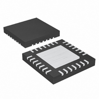
MAX8717ETI+ Maxim Integrated Products, MAX8717ETI+ Datasheet - Page 19

MAX8717ETI+
Manufacturer Part Number
MAX8717ETI+
Description
IC CNTRLR PWR SUP 28-TQFN
Manufacturer
Maxim Integrated Products
Datasheet
1.MAX8717ETI.pdf
(30 pages)
Specifications of MAX8717ETI+
Applications
Controller, Notebook Computers
Voltage - Input
4 ~ 26 V
Number Of Outputs
2
Voltage - Output
3.3V, 5V, 1 ~ 5.5 V
Operating Temperature
0°C ~ 85°C
Mounting Type
Surface Mount
Package / Case
28-TQFN Exposed Pad
Maximum Operating Temperature
+ 85 C
Mounting Style
SMD/SMT
Minimum Operating Temperature
- 40 C
Lead Free Status / RoHS Status
Lead free / RoHS Compliant
Connect FB1 and FB2 to V
output voltages (3.3V and 5V, respectively, for the
MAX8716/MAX8717/MAX8757, and 1.5V and 1.8V for
the MAX8756, respectively), set by a preset, internal
resistive voltage-divider connected between CSL_ and
analog ground. See Figure 5. Connect a resistive volt-
age-divider at FB_ between CSL_ and GND to adjust
the respective output voltage between 1V and 5.5V.
Choose R2 (resistance from FB to AGND) to be approx-
imately 10kΩ and solve for R1 (resistance from OUT to
FB) using the equation:
where V
The current-limit circuit uses differential current-sense
inputs (CSH_ and CSL_) to limit the peak inductor cur-
rent. If the magnitude of the current-sense signal
exceeds the current-limit threshold, the PWM controller
turns off the high-side MOSFET (Figure 3). At the next
rising edge of the internal oscillator, the PWM controller
does not initiate a new cycle unless the current-sense
signal drops below the current-limit threshold. The
actual maximum load current is less than the peak cur-
rent-limit threshold by an amount equal to half of the
Figure 5. Dual Mode Feedback Decoder
Interleaved High-Efficiency, Dual Power-Supply
AMPLIFIER
TO ERROR
CSL
FB_
FB
= 1V nominal.
Current-Limit Protection (ILIM_)
R
______________________________________________________________________________________
1
Adjustable/Fixed Output Voltages
=
2V
R
2
⎛
⎜
⎝
V
CC
V
OUT
Controllers for Notebook Computers
FB
FIXED OUTPUT
to enable the fixed SMPS
ADJUSTABLE
_
FB = V
(Dual-Mode Feedback)
_
OUTPUT
−
CC
1
⎞
⎟
⎠
inductor ripple current. Therefore, the maximum load
capability is a function of the current-sense resistance,
inductor value, switching frequency, and duty cycle
(V
In forced-PWM mode, the MAX8716/MAX8717/
MAX8756/MAX8757 also implement a negative current
limit to prevent excessive reverse inductor currents
when V
threshold is set to approximately -120% of the positive
current limit and tracks the positive current limit when
ILIM is adjusted.
Connect ILIM_ to V
adjust the current-limit threshold with an external resis-
tor-divider at ILIM_. Use a 2µA to 20µA divider current
for accuracy and noise immunity. The current-limit
threshold adjustment range is from 50mV to 200mV. In
the adjustable mode, the current-limit threshold voltage
equals precisely 1/10 the voltage seen at ILIM_. The
logic threshold for switchover to the 50mV default value
is approximately V
Carefully observe the PCB layout guidelines to ensure
that noise and DC errors do not corrupt the differential
current-sense signals seen by CSH_ and CSL_. Place
the IC close to the sense resistor with short, direct
traces, making a Kelvin-sense connection to the cur-
rent-sense resistor.
The DH_ and DL_ drivers are optimized for driving
moderate-sized high-side, and larger low-side power
MOSFETs. This is consistent with the low duty factor
seen in notebook applications, where a large V
V
(DH_) source and sink 2A, and the low-side gate dri-
vers (DL_) source 1.7A and sink 3.3A. This ensures
robust gate drive for high-current applications. The
DH_ floating high-side MOSFET drivers are powered by
diode-capacitor charge pumps at BST_ (Figure 6) while
the DL_ synchronous-rectifier drivers are powered
directly by the external 5V supply (V
Adaptive dead-time circuits monitor the DL_ and DH_ dri-
vers and prevent either FET from turning on until the other
is fully off. The adaptive driver dead-time allows operation
without shoot-through with a wide range of MOSFETs,
minimizing delays and maintaining efficiency. There must
be a low-resistance, low-inductance path from the DL_
and DH_ drivers to the MOSFET gates for the adaptive
dead-time circuits to work properly; otherwise, the sense
circuitry in the MAX8716/MAX8717/MAX8756/MAX8757
interprets the MOSFET gates as “off” while charge actually
remains. Use very short, wide traces (50 mils to 100 mils
wide if the MOSFET is 1in from the driver).
OUT
OUT
differential exists. The high-side gate drivers
/ V
OUT
IN
).
is sinking current. The negative current-limit
MOSFET Gate Drivers (DH_, DL_)
CC
CC
- 1V.
for the 50mV default threshold, or
DD
).
IN
19
-


