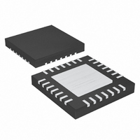
MAX8717ETI+ Maxim Integrated Products, MAX8717ETI+ Datasheet - Page 20

MAX8717ETI+
Manufacturer Part Number
MAX8717ETI+
Description
IC CNTRLR PWR SUP 28-TQFN
Manufacturer
Maxim Integrated Products
Datasheet
1.MAX8717ETI.pdf
(30 pages)
Specifications of MAX8717ETI+
Applications
Controller, Notebook Computers
Voltage - Input
4 ~ 26 V
Number Of Outputs
2
Voltage - Output
3.3V, 5V, 1 ~ 5.5 V
Operating Temperature
0°C ~ 85°C
Mounting Type
Surface Mount
Package / Case
28-TQFN Exposed Pad
Maximum Operating Temperature
+ 85 C
Mounting Style
SMD/SMT
Minimum Operating Temperature
- 40 C
Lead Free Status / RoHS Status
Lead free / RoHS Compliant
Interleaved High-Efficiency, Dual Power-Supply
Controllers for Notebook Computers
The internal pulldown transistor that drives DL_ low is
robust, with a 0.6Ω (typ) on-resistance. This helps pre-
vent DL_ from being pulled up due to capacitive cou-
pling from the drain to the gate of the low-side MOSFETs
when the inductor node (LX_) quickly switches from
ground to V
long inductive driver traces may require additional gate-
to-source capacitance to ensure fast-rising LX_ edges
do not pull up the low-side MOSFETs gate, causing
shoot-through currents. The capacitive coupling
between LX_ and DL_ created by the MOSFET’s gate-to-
drain capacitance (C
(C
exceed the following minimum threshold:
Variation of the threshold voltage may cause problems
in marginal designs. Alternatively, adding a resistor
less than 10Ω in series with BST_ may remedy the
problem by increasing the turn-on time of the high-side
MOSFET without degrading the turn-off time (Figure 6).
Figure 6. Optional Gate-Driver Circuitry
20
ISS
______________________________________________________________________________________
MAX8716
MAX8717
MAX8756
MAX8757
- C
(R
THE SWITCHING-NODE RISE TIME.
(C
COUPLING THAT CAN CAUSE SHOOT-THROUGH CURRENTS.
BST
NL
RSS
)* OPTIONAL—THE CAPACITOR REDUCES LX TO DL CAPACITIVE
)* OPTIONAL—THE RESISTOR LOWERS EMI BY DECREASING
V
IN
), and additional board parasitics should not
DD
. Applications with high input voltages and
PGND
V
BST
GS TH
V
DH
DD
LX
DL
(
RSS
)
(R
>
BST
), gate-to-source capacitance
(C
C
V
BST
NL
)*
IN
)*
⎛
⎜
⎝
C
C
D
RSS
C
ISS
BST
BYP
⎞
⎟
⎠
N
N
H
L
INPUT (V
L
IN
)
PGOOD_ is the open-drain output of a comparator that
continuously monitors each SMPS output voltage for
overvoltage and undervoltage conditions. PGOOD_ is
actively held low in shutdown (ON_ = GND), soft-start,
and soft-shutdown. Once the analog soft-start termi-
nates, PGOOD_ becomes high impedance as long as
the output is above 90% of the nominal regulation volt-
age set by FB_. PGOOD_ goes low once the output
drops 10% below its nominal regulation point, an output
overvoltage fault occurs, or ON_ is pulled low. For a
logic-level PGOOD_ output voltage, connect an exter-
nal pullup resistor between PGOOD_ and +5V or +3.3V.
A 100kΩ pullup resistor works well in most applications.
If the output voltage of either SMPS rises above 115%
of its nominal regulation voltage, the corresponding
controller sets its overvoltage fault latch, pulls PGOOD_
low, and forces DL_ high for the corresponding SMPS
controller. The other controller is not affected. If the
condition that caused the overvoltage persists (such as
a shorted high-side MOSFET), the battery fuse will
blow. Cycle V
overvoltage fault latch and restart the SMPS controller.
Figure 7. Power-Good and Fault Protection
POWER-GOOD
INT REF_
0.9 x
CC
Power-Good Output (PGOOD_)
(MAX8716/MAX8717/MAX8756 Only)
below 1V or toggle ON_ to clear the
INT REF_
1.15 x
Output Overvoltage Protection
PROTECTION
FAULT
INT REF_
0.7 x
Fault Protection
LATCH
FAULT
INTERNAL FB
TIMER
POR
POWER-
GOOD
FAULT


