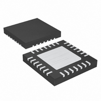
MAX8717ETI+ Maxim Integrated Products, MAX8717ETI+ Datasheet - Page 21

MAX8717ETI+
Manufacturer Part Number
MAX8717ETI+
Description
IC CNTRLR PWR SUP 28-TQFN
Manufacturer
Maxim Integrated Products
Datasheet
1.MAX8717ETI.pdf
(30 pages)
Specifications of MAX8717ETI+
Applications
Controller, Notebook Computers
Voltage - Input
4 ~ 26 V
Number Of Outputs
2
Voltage - Output
3.3V, 5V, 1 ~ 5.5 V
Operating Temperature
0°C ~ 85°C
Mounting Type
Surface Mount
Package / Case
28-TQFN Exposed Pad
Maximum Operating Temperature
+ 85 C
Mounting Style
SMD/SMT
Minimum Operating Temperature
- 40 C
Lead Free Status / RoHS Status
Lead free / RoHS Compliant
If the output voltage of either SMPS falls below 70% of
its regulation voltage, the corresponding controller sets
its undervoltage fault latch, pulls PGOOD_ low, and
begins soft-shutdown for the corresponding SMPS con-
troller by pulsing DL_. DH_ remains off during the soft-
shutdown sequence initiated by an unvervoltage fault.
The other controller is not affected. After soft-shutdown
has completed, the MAX8716/MAX8717/MAX8756/
MAX8757 force DL_ high and DH_ low. Cycle V
below 1V or toggle ON_ to clear the undervoltage fault
latch and restart the SMPS controller.
Power-on reset (POR) occurs when V
approximately 2V, resetting the fault latch and prepar-
ing the PWM for operation. V
(UVLO) circuitry inhibits switching, forces PGOOD_
low, and forces the DL_ gate drivers low.
If V
while ON_ is high, the MAX8716/MAX8717/MAX8756/
MAX8757 immediately force DH_ and DL_ low on both
controllers. The output discharges to 0V at a rate
dependent on the load and the total output capaci-
tance. This prevents negative output voltages, eliminat-
ing the need for a Schottky diode to GND at the output.
The MAX8716/MAX8717/MAX8756/MAX8757 feature a
thermal fault-protection circuit. When the junction tem-
perature rises above +160°C, a thermal sensor sets the
fault latches, pulls PGOOD low, and shuts down both
SMPS controllers using the soft-shutdown sequence
(see the Sort-Start and Soft-Shutdown section). Cycle
V
latches and restart the controllers after the junction
temperature cools by 15°C.
Firmly establish the input voltage range and maximum
load current before choosing a switching frequency
and inductor operating point (ripple-current ratio). The
primary design trade-off lies in choosing a good switch-
ing frequency and inductor operating point, and the fol-
lowing four factors dictate the rest of the design:
• Input Voltage Range. The maximum value (V
CC
Interleaved High-Efficiency, Dual Power-Supply
must accommodate the worst-case, high AC-adapter
voltage. The minimum value (V
for the lowest battery voltage after drops due to con-
nectors, fuses, and battery selector switches. If there
is a choice at all, lower input voltages result in better
efficiency.
CC
below 1V or toggle ON1 and ON2 to clear the fault
drops low enough to trip the UVLO comparator
______________________________________________________________________________________
Output Undervoltage Protection
Design Procedure
Controllers for Notebook Computers
Thermal Fault Protection
CC
IN(MIN)
V
undervoltage-lockout
CC
POR and UVLO
CC
) must account
rises above
IN(MAX)
CC
)
• Maximum Load Current. There are two values to
• Switching Frequency. This choice determines the
• Inductor Operating Point. This choice provides
The switching frequency and inductor operating point
determine the inductor value as follows:
For example: I
f
Find a low-loss inductor having the lowest possible DC
resistance that fits in the allotted dimensions. Most
inductor manufacturers provide inductors in standard
values, such as 1.0µH, 1.5µH, 2.2µH, 3.3µH, etc. Also
OSC
consider. The peak load current (I
mines the instantaneous component stresses and fil-
tering requirements and thus drives output capacitor
selection, inductor saturation rating, and the design
of the current-limit circuit. The continuous load cur-
rent (I
drives the selection of input capacitors, MOSFETs,
and other critical heat-contributing components.
basic trade-off between size and efficiency. The
optimal frequency is largely a function of maximum
input voltage, due to MOSFET switching losses that
are proportional to frequency and V
mum frequency is also a moving target, due to rapid
improvements in MOSFET technology that are mak-
ing higher frequencies more practical.
trade-offs between size vs. efficiency and transient
response vs. output ripple. Low inductor values pro-
vide better transient response and smaller physical
size, but also result in lower efficiency and higher
output ripple due to increased ripple currents. The
minimum practical inductor value is one that causes
the circuit to operate at the edge of critical conduc-
tion (where the inductor current just touches zero
with every cycle at maximum load). Inductor values
lower than this grant no further size-reduction bene-
fit. The optimum operating point is usually found
between 20% and 50% ripple current. When pulse-
skipping (SKIP low and light loads), the inductor
value also determines the load-current value at
which PFM/PWM switchover occurs.
= 300kHz, 30% ripple current or LIR = 0.3:
LOAD
L
=
12
) determines the thermal stresses and thus
L
LOAD(MAX)
V
=
×
5
V
V
300
IN OSC LOAD MAX
×
V
ƒ
OUT IN
(
kHz
12
V
(
= 5A, V
I
×
V
−
5
5
A
V
−
)
×
Inductor Selection
V
(
0 3
OUT
IN
.
= 12V, V
=
)
)
LIR
LOAD(MAX)
6 50
.
IN
μ
2
H
. The opti-
OUT
) deter-
= 5V,
21


