ISL6423ERZ-T Intersil, ISL6423ERZ-T Datasheet - Page 13
ISL6423ERZ-T
Manufacturer Part Number
ISL6423ERZ-T
Description
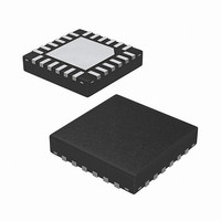
IC VREG SGL LNB W/I2C 24-QFN
Manufacturer
Intersil
Datasheet
1.ISL6423ERZ.pdf
(16 pages)
Specifications of ISL6423ERZ-T
Applications
Converter, Satellite Set-Top Box Designs
Voltage - Input
8 ~ 14 V
Number Of Outputs
1
Voltage - Output
13.3 ~ 18.3 V, 14.3 ~ 19.3 V
Operating Temperature
-20°C ~ 85°C
Mounting Type
Surface Mount
Package / Case
24-VQFN
Lead Free Status / RoHS Status
Lead free / RoHS Compliant
Available stocks
Company
Part Number
Manufacturer
Quantity
Price
Company:

Part Number:
ISL6423ERZ-T
Manufacturer:
JMICRON
Quantity:
256


NOTE: X indicates “Read Only” and is a “Don’t Care” for the Write mode.
Received Data (
The ISL6423 can provide to the master a copy of the system
register information via the I
mode is Master activated by sending the chip address with
R/W bit set to 1. At the following Master generated clock bits,
the ISL6423 issues a byte on the SDA data bus line (MSB
transmitted first).
At the ninth clock bit the MCU master can:
• Acknowledge the reception, starting in this way the
• Not acknowledge, stopping the read mode
The read only bits of the register SR1 convey diagnostic
information about the ISL6423, as indicated in the Table 7.
Power–On I
The I
at power-on. The I
logic signal from the UVLO circuit. This signal will go HIGH
when chip power is OK. As long as this signal is LOW, the
interface will not respond to any I
system register SR1 thru SR4 are all initialized to zero, thus
keeping the power blocks disabled. Once the VCC rises
above UVLO, the POWER OK signal to the I
high, and the I
can be configured by the main microprocessor. About
400mV of hysteresis is provided in the UVLO threshold to
avoid false triggering of the power-on reset circuit. (I
comes up with EN = 0; EN goes HIGH at the same time as
(or later than) all other I
valid).
SR4H
transmission of another byte from the ISL6423.
communication.
0
0
0
0
0
0
0
0
0
0
0
0
0
0
2
C interface built into the ISL6423 is automatically reset
SR4M
1
1
1
1
1
1
1
1
1
1
1
1
1
1
2
2
C Interface Reset
C interface becomes operative and the SR’s
2
I
SR4L
2
C interface block will receive a power OK
C
1
1
1
1
1
1
1
1
1
1
1
1
1
1
bus READ MODE)
2
C data for that PWM becomes
2
13
EN
C bus in read mode. The read
1
1
1
1
1
1
1
1
1
1
1
1
1
0
2
C commands and the
TABLE 10. CONTROL REGISTER SR4 CONFIGURATION
X
X
X
X
X
X
X
X
X
X
X
X
X
X
X
2
C is asserted
X
X
X
X
X
X
X
X
X
X
X
X
X
X
X
2
C
VTOP
X
0
0
0
1
1
0
0
1
1
0
0
1
1
ISL6423
VBOT
X
0
0
1
0
1
0
1
0
1
0
1
0
1
ADDR0 and ADDR1 Pins
Connecting these pin to GND the chip I
is 0001000, but, it is possible to choose between four
different addresses by setting these pins to the logic levels
indicated in Table 11.
SR4 is selected
VSPEN = SELVTOP = 0, Vout1 = 13V, Vboost1 = 13V + Vdrop
VSPEN = SELVTOP = 0, Vout1 = 14V, Vboost1 = 14V + Vdrop
VSPEN = SELVTOP = 0, Vout1 = 13V, Vboost1 = 13V + Vdrop
VSPEN = SELVTOP = 0, Vout1 = 14V, Vboost1 = 14V + Vdrop
VSPEN = 0, SELVTOP = 1, Vout1 = 18V, Vboost1 = 18V + Vdrop
VSPEN = 0, SELVTOP = 1, Vout1 = 18V, Vboost1 = 18V + Vdrop
VSPEN = 0, SELVTOP = 1, Vout1 = 19V, Vboost1 = 19V + Vdrop
VSPEN = 0, SELVTOP = 1, Vout1 = 19V, Vboost1 = 19V + Vdrop
VSPEN = 1, SELVTOP = X Vout1 = 13V, Vboost1 = 13V + Vdrop
VSPEN = 1, SELVTOP = X Vout1 = 14V, Vboost1 = 14V + Vdrop
VSPEN = 1, SELVTOP = X Vout1 = 18V, Vboost1 = 18V + Vdrop
VSPEN = 1, SELVTOP = X Vout1 = 19V, Vboost1 = 19V + Vdrop
PWM and Linear for channel 1 disabled
TABLE 11. ADDRESS PIN CHARACTERISTICS
V
V
V
V
ADDR
ADDR
ADDR
ADDR
V
-1 “0001000”
-2 “0001001”
-3 “0001010”
-4 “0001011”
ADDR
FUNCTION
ADDR1
0
0
1
1
2
C interface address
ADDR0
December 5, 2008
0
1
0
1
FN9191.2
Related parts for ISL6423ERZ-T
Image
Part Number
Description
Manufacturer
Datasheet
Request
R

Part Number:
Description:
Single Output Lnb Supply And Control Voltage Regulator With I2c Interface For Advanced Satellite Set-top Box Designs, Diseqc 2.0 Compatible
Manufacturer:
Intersil Corporation
Datasheet:
Part Number:
Description:
Intersil Corporation [CMOS Serial Controller Interface]
Manufacturer:
Intersil Corporation
Datasheet:
Part Number:
Description:
Manufacturer:
Intersil Corporation
Datasheet:
Part Number:
Description:
357-036-542-201 CARDEDGE 36POS DL .156 BLK LOPRO
Manufacturer:
Intersil Corporation
Datasheet:
Part Number:
Description:
1024-Word x 4-Bit LSI Static RAM
Manufacturer:
Intersil Corporation
Datasheet:
Part Number:
Description:
General Purpose NPN Transistor Arrays FN341.4
Manufacturer:
Intersil Corporation
Datasheet:
Part Number:
Description:
CMOS 16-Bit Microprocessor
Manufacturer:
Intersil Corporation
Datasheet:
Part Number:
Description:
Manufacturer:
Intersil Corporation
Datasheet:
Part Number:
Description:
Manufacturer:
Intersil Corporation
Datasheet:
Part Number:
Description:
Manufacturer:
Intersil Corporation
Datasheet:
Part Number:
Description:
Manufacturer:
Intersil Corporation
Datasheet:
Part Number:
Description:
CMOS 6-Bit Latch and Decoder Memory Interfaces
Manufacturer:
Intersil Corporation
Datasheet:
Part Number:
Description:
CA3046General Purpose NPN Transistor Arrays
Manufacturer:
Intersil Corporation
Datasheet:
Part Number:
Description:
Manufacturer:
Intersil Corporation
Datasheet:
Part Number:
Description:
TR909 DLC/FLC SLIC with Low Power Standby
Manufacturer:
Intersil Corporation
Datasheet: