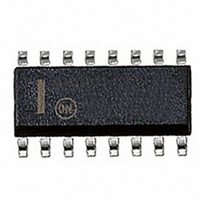
CS5165AGDWR16G ON Semiconductor, CS5165AGDWR16G Datasheet - Page 6

CS5165AGDWR16G
Manufacturer Part Number
CS5165AGDWR16G
Description
IC CTRLR BUCK SYNC 5BIT 16-SOIC
Manufacturer
ON Semiconductor
Datasheet
1.CS5165AGDWR16G.pdf
(18 pages)
Specifications of CS5165AGDWR16G
Applications
Controller, Intel Pentium® II
Voltage - Input
8 ~ 14 V
Number Of Outputs
2
Voltage - Output
1.34 ~ 2.09 V, 2.14 ~ 3.54 V
Operating Temperature
0°C ~ 70°C
Mounting Type
Surface Mount
Package / Case
16-SOIC (0.300", 7.5mm Width)
Mounting Style
SMD/SMT
Lead Free Status / RoHS Status
Lead free / RoHS Compliant
Available stocks
Company
Part Number
Manufacturer
Quantity
Price
Part Number:
CS5165AGDWR16G
Manufacturer:
ON/安森美
Quantity:
20 000
PWRGD
ENABLE
PACKAGE PIN DESCRIPTION
COMP
LGND
V
V
V
PACKAGE PIN #
V
V
V
SS
ID0
ID1
ID2
ID3
ID4
FB
1, 2, 3, 4, 6
SOIC−16
−8.5%
10
12
13
14
15
16
11
5
7
8
9
1.25 V
5 BIT
DAC
20 k
+
V
CC
+8.5%
−
65 ms
Delay
PIN SYMBOL
Enable
Comparator
−
7.0 mA
+
−
V
GATE(H)
ENABLE
GATE(L)
PWRGD
Error Amplifier
ID0
COMP
PGND
LGND
+
C
V
V
SS
OFF
−V
CC
FB
+
−
ID4
1.0 V
Circuit Bias
Voltage ID DAC input pins. These pins are internally pulled up to 5.0 V if left open. V
the DAC range. When V
with 100 mV increments. When V
to 2.09 V with 50 mV increments.
Soft−Start Pin. A capacitor from this pin to LGND sets the Soft−Start and fault timing.
Off−Time Capacitor Pin. A capacitor from this pin to LGND sets both the normal and extended off
time.
Output Enable Input. This pin is internally pulled up to 1.8 V. A logic Low (< 0.8) on this pin
disables operation and places the CS5165A into a low current sleep mode.
Input Power Supply Pin.
High Side Switch FET driver pin.
High current ground for the GATE(H) and GATE(L) pins.
Low Side Synchronous FET driver pin.
Power Good Output. Open collector output drives low when V
ENABLE input is low.
Reference ground. All control circuits are referenced to this pin.
Error Amp output. PWM Comparator reference input. A capacitor to LGND provides Error Amp
compensation.
Error Amp, PWM Comparator, and Low V
PWM
Comparator
2.0 mA
60 mA
+
+
−
−
V
Comparator
FB
5.0 V
Figure 2. Block Diagram
Low
http://onsemi.com
CS5165A
V
PWM COMP
CC
Blanking
ID4
Monitor
6
is high (logic one), the Error Amp reference range is 2.14 V to 3.45 V
2.5 V
0.7 V
Extended
Off−Time
Off−Time
Timeout
Timeout
Maximum
Normal
On−Time
ID4
+
+
Timeout
−
−
is low (logic zero), the Error Amp reference voltage 1.34 V
SS Low
Comparator
SS High
Comparator
FB
FUNCTION
+
−
Time−Out
Comparator feedback input.
(30 ms)
Timer
Off−Time
Timeout
R
S
FAULT
3.95 V
3.87V
Latch
Q
Q
S
R
FAULT
FAULT
PWM
Latch
FB
Edge Triggered
Q
Q
is out of regulation. Active when
GATE(H) = ON
GATE(H) = OFF
S
One Shot
R
C
OFF
Q
V
PGND
V
CC1
CC
ID4
selects
V
V
V
C
PGND
GATE(H)
GATE(L)
CC
OFF


