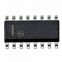
CS5165AGDWR16G ON Semiconductor, CS5165AGDWR16G Datasheet - Page 9

CS5165AGDWR16G
Manufacturer Part Number
CS5165AGDWR16G
Description
IC CTRLR BUCK SYNC 5BIT 16-SOIC
Manufacturer
ON Semiconductor
Datasheet
1.CS5165AGDWR16G.pdf
(18 pages)
Specifications of CS5165AGDWR16G
Applications
Controller, Intel Pentium® II
Voltage - Input
8 ~ 14 V
Number Of Outputs
2
Voltage - Output
1.34 ~ 2.09 V, 2.14 ~ 3.54 V
Operating Temperature
0°C ~ 70°C
Mounting Type
Surface Mount
Package / Case
16-SOIC (0.300", 7.5mm Width)
Mounting Style
SMD/SMT
Lead Free Status / RoHS Status
Lead free / RoHS Compliant
Available stocks
Company
Part Number
Manufacturer
Quantity
Price
Part Number:
CS5165AGDWR16G
Manufacturer:
ON/安森美
Quantity:
20 000
capacitor begins charging. The GATE(H) output will remain
on, enabling the NFET switch, until terminated by either the
PWM comparator, or the maximum on time timer.
output voltage achieves the 1.0 V level, the pulse is terminated.
The GATE(H) pin drives low, and the GATE(L) pin drives high
for the duration of the extended off time. This time is set by the
time out timer and is approximately equal to the maximum on
time, resulting in a 50% duty cycle. The GATE(L) pin will then
drive low, the GATE(H) pin will drive high, and the cycle
repeats.
present at the COMP pin, regulation has been achieved and
normal off time will ensue. The PWM comparator terminates
the switch on time, with off time set by the C
V
ensure the regulator output voltage tracks the output of the
error amplifier.
final levels, providing a controlled turn on of the regulator
output. Regulator turn on time is determined by the COMP
capacitor charging to its final value. Its voltage is limited by the
Soft−Start COMP clamp and the voltage on the Soft−Start pin.
Power Supply Sequencing
startup conditions, regardless of the 12 V and 5.0 V supply
power up sequencing. The turn on slew rates of the 12 V and
5.0 V power supplies can be varied over wide ranges without
affecting the output voltage or causing detrimental effects to
the buck regulator.
Voltages. Extended Off Time is Followed by Normal
2
If the maximum on time is exceeded before the regulator
When regulator output voltage achieves the 1.0 V level
The Soft−Start and COMP capacitors will charge to their
The CS5165A offers inherent protection from undefined
Off Time Operation when Output Voltage Achieves
Trace 1− Regulator Output Voltage (1.0 V/div.)
Trace 2− Inductor Switching Node (2.0 V/div.)
Trace 3− 12 V Input (V
Trace 4− 5.0 V Input (1.0 V/div.)
control loop will adjust switch duty cycle as required to
Response to Increasing 12 V and 5.0 V Input
Figure 10. Demonstration Board Startup in
Regulation to the Error Amplifier Output.
CC
) (5.0 V/div.)
M 250 ms
OFF
capacitor. The
http://onsemi.com
CS5165A
9
Normal Operation
set by the C
V
in regulator switching frequency, duty cycle, and output
ripple in response to changes in load and line. Output voltage
ripple will be determined by inductor ripple current working
and the ESR of the output capacitors (see Figures 13 and 14).
2
Figure 11. Demonstration Board Startup Waveforms
Trace 1− Soft−Start Pin (2.0 V/div.)
Trace 2− COMP PIn (error amplifier output) (1.0 V/div.)
Trace 4− Regulator Output Voltage (1.0 V/div.)
During normal operation, switch off time is constant and
Trace 1− Regulator Output Voltage (1.0 V/div.)
Trace 2− Inductor Switching Node (5.0 V/div.)
control loop to maintain regulation. This results in changes
Figure 12. Demonstration Board Enable Startup
OFF
capacitor. Switch on time is adjusted by the
Waveforms
M 10.0 ms


