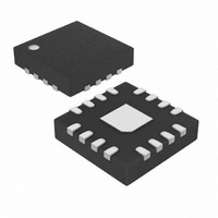
MAX8506ETE+ Maxim Integrated Products, MAX8506ETE+ Datasheet - Page 7

MAX8506ETE+
Manufacturer Part Number
MAX8506ETE+
Description
IC DC-DC CONV PWM 16-TQFN
Manufacturer
Maxim Integrated Products
Datasheet
1.MAX8506ETET.pdf
(11 pages)
Specifications of MAX8506ETE+
Applications
Converter, WCDMA
Voltage - Input
2.6 ~ 5.5 V
Number Of Outputs
1
Voltage - Output
0.4 ~ 3.4 V
Operating Temperature
-40°C ~ 85°C
Mounting Type
Surface Mount
Package / Case
16-TQFN Exposed Pad
Lead Free Status / RoHS Status
Lead free / RoHS Compliant
The MAX8506/MAX8507/MAX8508 use a fixed-frequen-
cy, current-mode and PWM controller capable of achiev-
ing 100% duty cycle. Current-mode feedback provides
cycle-by-cycle current limiting and superior load and line
response, as well as overcurrent protection for the inter-
nal MOSFET and rectifier. A comparator at the P-channel
MOSFET switch detects overcurrent at 1.25A.
During PWM operation, the MAX8506/MAX8507/
MAX8508 regulate the output voltage by switching at a
constant frequency and then modulating the duty cycle
with PWM control. The error-amp output, the main
switch current-sense signal, and the slope-compensa-
tion ramp are all summed using a PWM comparator.
The comparator modulates the output power by adjust-
ing the peak inductor current during the first half of
each cycle based on the output-error voltage. The
MAX8506/MAX8507/MAX8508 have relatively low AC
loop gain coupled with a high-gain integrator to enable
the use of a small and low-valued output filter capaci-
tor. The resulting load regulation is 0.1% at 0 to 600mA.
Connecting SKIP to GND enables normal operation. This
allows automatic PWM control at medium and heavy
loads and skip mode at light loads to improve efficiency
and reduce quiescent current to 180µA. Operating in
normal mode allows the MAX8506/MAX8507/MAX8508
to pulse skip when the peak inductor current drops
below 90mA. During skip operation, the MAX8506/
MAX8507/MAX8508 switch only as needed to service
the load, reducing the switching frequency and associat-
ed losses in the internal switch and synchronous rectifier.
There are three steady-state operating conditions for
the MAX8506/MAX8507/MAX8508 in normal mode:
1) The device performs in continuous conduction for
heavy loads in a manner identical to forced-PWM
mode. 2) The inductor current becomes discontinuous
at medium loads, requiring the synchronous rectifier to
be turned off before the end of a cycle as the inductor
current reaches zero. 3) The device enters into skip
mode when the converter output voltage exceeds its
regulation limit before the inductor current reaches its
skip threshold level.
During skip mode, a switching cycle initiates when the
output voltage has dropped out of regulation. The P-
channel MOSFET switch turns on and conducts current
to the output-filter capacitor and load until the inductor
current reaches the pulse-skipping current threshold.
Bypass FET for WCDMA and cdmaOne Handsets
PWM Step-Down DC-DC Converters with 75m Ω Ω
_______________________________________________________________________________________
Normal-Mode Operation
PWM Control
Then the main switch turns off and the magnetic field in
the inductor collapses while current flows through the
synchronous rectifier to the output filter capacitor and
the load. The synchronous rectifier is turned off when
the inductor current reaches zero. The MAX8506/
MAX8507/MAX8508 wait until the skip comparator
senses a low output voltage again.
Connect SKIP to BATT for forced-PWM operation.
Forced-PWM operation is desirable in sensitive RF and
data-acquisition applications to ensure that switching
harmonics do not interfere with sensitive IF and data-
sampling frequencies. A minimum load is not required
during forced-PWM operation since the synchronous
rectifier passes reverse-inductor current as needed to
allow constant-frequency operation with no load. Forced-
PWM operation uses higher supply current with no load
(1.75mA typ) compared to skip mode (180µA typ).
The maximum on-time can exceed one internal oscilla-
tor cycle, which permits operation at 100% duty cycle.
Near dropout, cycles can be skipped, reducing switch-
ing frequency. However, voltage ripple remains small
because the current ripple is still low. As the input volt-
age drops even further, the duty cycle increases until
the internal P-channel MOSFET stays on continuously.
Dropout voltage at 100% duty cycle is the output cur-
rent multiplied by the sum of the internal PMOS on-
resistance (400mΩ typ) and the inductor resistance.
For lower dropout, use the high-power bypass mode
(75mΩ typ).
A high-power bypass mode is available for use when a
PA transmits at high power. This mode connects OUT
to BATT through the bypass PFET. Additionally, the
PWM buck converter is forced into 100% duty cycle to
further reduce dropout. The dropout in the bypass
PFET equals the load current multiplied by the on-resis-
tance (75Ω typ) in parallel with the buck converter and
inductor dropout resistance.
The MAX8506/MAX8507/MAX8508 do not operate with
battery voltages below the UVLO threshold of 2.35V
(typ). The output remains off until the supply voltage
exceeds the UVLO threshold. This guarantees the
integrity of the output voltage regulation.
100% Duty-Cycle Operation and Dropout
Undervoltage Lockout (UVLO)
High-Power Bypass Mode
Forced-PWM Operation
7


