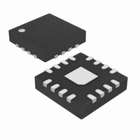
MAX8506ETE+ Maxim Integrated Products, MAX8506ETE+ Datasheet - Page 8

MAX8506ETE+
Manufacturer Part Number
MAX8506ETE+
Description
IC DC-DC CONV PWM 16-TQFN
Manufacturer
Maxim Integrated Products
Datasheet
1.MAX8506ETET.pdf
(11 pages)
Specifications of MAX8506ETE+
Applications
Converter, WCDMA
Voltage - Input
2.6 ~ 5.5 V
Number Of Outputs
1
Voltage - Output
0.4 ~ 3.4 V
Operating Temperature
-40°C ~ 85°C
Mounting Type
Surface Mount
Package / Case
16-TQFN Exposed Pad
Lead Free Status / RoHS Status
Lead free / RoHS Compliant
An N-channel synchronous rectifier operates during the
second half of each switching cycle (off-time). When
the inductor current falls below the N-channel current-
comparator threshold or when the PWM reaches the
end of the oscillator period, the synchronous rectifier
turns off. This prevents reverse current from the output
to the input in pulse-skipping mode. During PWM oper-
ation, the NEGLIM threshold adjusts to permit reverse
current during light loads. This allows regulation with a
constant switching frequency and eliminates minimum
load requirements for fixed-frequency operation.
Drive SHDN to GND to place the MAX8506/MAX8507/
MAX8508 in shutdown mode. In shutdown, the refer-
ence, control circuitry, internal switching MOSFET, and
synchronous rectifier turn off and the output becomes
high impedance. Input current falls to 0.1µA (typ) dur-
ing shutdown mode. Drive SHDN high to enable the IC.
The MAX8506/MAX8507/MAX8508 use several internal
current-sense comparators. In PWM operation, the PWM
comparator terminates the cycle-by-cycle on-time and
provides improved load and line response. A second cur-
rent-sense comparator used across the P-channel switch
controls entry into skip mode. A third current-sense com-
parator monitors current through the internal N-channel
MOSFET to prevent excessive reverse currents and
determine when to turn off the synchronous rectifier. A
fourth comparator used at the P-channel MOSFET
detects overcurrent. A fifth comparator used at the
bypass P-channel MOSFET detects overcurrent in the
HP mode or at dropout. This protects the system, exter-
nal components, and internal MOSFETs under overload
conditions.
The MAX8506/MAX8507 are optimized for highest sys-
tem efficiency when applying power to a linear PA in
CDMA handsets. When transmitting at less than full
power, the supply voltage to the PA is lowered in many
steps from 3.4V to as low as 0.4V to greatly reduce bat-
tery current (see the Typical Application Circuits). The
use of DC-DC converters such as the MAX8506/
MAX8507 dramatically extends talk time in these appli-
cations.
PWM Step-Down DC-DC Converters with 75m Ω Ω
Bypass FET for WCDMA and cdmaOne Handsets
8
_______________________________________________________________________________________
Applications Information
Using a DAC (MAX8506/MAX8507)
Current-Sense Comparators
Setting the Output Voltage
Synchronous Rectification
Shutdown Mode
The MAX8506/MAX8507s’ output voltage is dynamically
adjustable from 0.4V to 3.4V by the use of the REFIN
input. The gain from V
1.76 (MAX8506) or 2.00 (MAX8507). V
ed during operation by driving REFIN with an external
DAC. The MAX8506/MAX8507 output responds to full-
scale change in voltage and current in less than 30µs.
The MAX8508 is intended for two-step V
applications where high efficiency is a priority. Select
an output voltage between 0.75V and 3.4V by connect-
ing FB to a resistive-divider between the output and
GND (see the MAX8508 Typical Application Circuit).
Select feedback resistor R2 in the 5kΩ to 50kΩ range.
R1 is then given by:
where V
Capacitor ESR is a major contributor to input ripple in
high-frequency DC-DC converters. Ordinary aluminum-
electrolytic capacitors have high ESR and should be
avoided. Low-ESR tantalum or polymer capacitors are
better and provide a compact solution for space-con-
strained surface-mount designs. Ceramic capacitors
have the lowest overall ESR.
The input filter capacitor reduces peak currents and
noise at the input voltage source. Connect a low-ESR
bulk capacitor (2.2µF to 10µF) to the input. Select this
bulk capacitor to meet the input ripple requirements
and voltage rating rather than capacitance value. Use
the following equation to calculate the maximum RMS
input current:
The MAX8506/MAX8507/MAX8508 are externally com-
pensated by placing a resistor and a capacitor (see the
Typical Application Circuits, R
COMP to GND. An additional capacitor (C
required from COMP to GND if high-ESR output capaci-
tors are used. The C
from the transimpedance amplifier, averaging output
FB
I
RMS
= 0.75V.
=
R
1
I
OUT
V
=
IN
Compensation, Stability, and
Using External Divider (MAX8508)
R
2
×
C
Input Capacitor Selection
REFIN
×
capacitor integrates the current
V
OUT
V
V
OUT
to V
FB
×
C
(
V
and C
OUT
−
Output Capacitor
IN
1
−
OUT
V
is internally set to
OUT
C
) in series from
can be adjust-
)
CC
f
) may be
control


