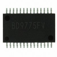
BD9775FV-E2 Rohm Semiconductor, BD9775FV-E2 Datasheet - Page 12

BD9775FV-E2
Manufacturer Part Number
BD9775FV-E2
Description
IC REG SW STEP DOWN HE 28-SSOP
Manufacturer
Rohm Semiconductor
Type
Step-Down (Buck)r
Specifications of BD9775FV-E2
Internal Switch(s)
No
Synchronous Rectifier
Yes
Number Of Outputs
2
Current - Output
400mA
Frequency - Switching
100kHz
Voltage - Input
6 ~ 30 V
Operating Temperature
-40°C ~ 85°C
Mounting Type
Surface Mount
Package / Case
28-SSOP
Power - Output
640mW
Mounting Style
SMD/SMT
Lead Free Status / RoHS Status
Lead free / RoHS Compliant
Voltage - Output
-
Lead Free Status / Rohs Status
Lead free / RoHS Compliant
Other names
BD9775FV-E2TR
© 2011 ROHM Co., Ltd. All rights reserved.
BD9775FV
www.rohm.com
13) If Gate capacitance of P-channel MOSFET or resistance placed on
14) IC pin input
(PINA)
N
P
Gate is large, and the time from beginning of Gate switching to the end of Drain’s (tsw), is long, it may not start up due to
the OCP malfunction. To avoid it, select MOSFET or adjust resistance as tsw becomes less than 270nsec.
This monolithic IC contains P+ isolation and PCB layers between adjacent elements in order to keep them isolated.
P/N junctions are formed at the intersection of these P layers with the N layers of other elements to create a variety of
parasitic elements. For example, when a resistor and transistor are connected to pins as shown in following chart,
The formation of parasitic elements as a result of the relationships of the potentials of different pins is an inevitable result
of the IC's architecture. The operation of parasitic elements can cause interference with circuit operation as well as IC
malfunction and damage. For these reasons, it is necessary to use caution so that the IC is not used in a way that will
trigger the operation of parasitic elements, such as by the application of voltages lower than the GND (PCB) voltage to
input and output pins.
P
○the P/N junction functions as a parasitic diode when GND > (Pin A) for the resistor or GND > (Pin B) for the
○Similarly, when GND > (Pin B) for the transistor (NPN), the parasitic diode described above combines with the N
+
transistor (NPN).
layer of other adjacent elements to operate as a parasitic NPN transistor.
Resistor
N
P
GND
Parasitic element
P
+
(PINB)
N
Parasitic element or transistor
P
+
C
Transistor (NPN)
P substrate
GATE
DRAIN
N
B
GND
P
E
Fig.15
Fig.16
12/14
P
+
N
tsw
Parasitic element or transistor
(PINB)
B
C
E
GND
(PINA)
Parasitic element
Technical Note
2011.05 - Rev.A


