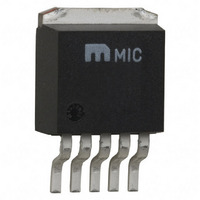
MIC2171WU Micrel Inc, MIC2171WU Datasheet - Page 6

MIC2171WU
Manufacturer Part Number
MIC2171WU
Description
IC REG SW 100KHZ 2.5A TO263-5
Manufacturer
Micrel Inc
Type
Step-Down (Buck), Step-Up (Boost), Inverting, Cukr
Datasheet
1.MIC2171WU_TR.pdf
(12 pages)
Specifications of MIC2171WU
Internal Switch(s)
Yes
Synchronous Rectifier
No
Number Of Outputs
1
Current - Output
2.5A
Frequency - Switching
100kHz
Voltage - Input
3 ~ 40 V
Operating Temperature
-40°C ~ 85°C
Mounting Type
Surface Mount
Package / Case
D²Pak, TO-263 (5 leads + tab)
Power - Output
1.3W
Number Of Pwm Outputs
1
On/off Pin
No
Adjustable Output
No
Switching Freq
112KHz
Operating Supply Voltage (max)
40V
Output Current
2.5A
Output Voltage
65V
Synchronous Pin
No
Operating Temperature Classification
Industrial
Mounting
Surface Mount
Pin Count
5 +Tab
Package Type
TO-263
Duty Cycle
95%
Lead Free Status / RoHS Status
Lead free / RoHS Compliant
Voltage - Output
-
Lead Free Status / RoHS Status
Compliant, Lead free / RoHS Compliant
Other names
576-1063
Available stocks
Company
Part Number
Manufacturer
Quantity
Price
Company:
Part Number:
MIC2171WU
Manufacturer:
MIC
Quantity:
740
Application Information
Soft Start
A diode-coupled capacitor from COMP to circuit ground
slows the output voltage rise at turn on (Figure 3).
The additional time it takes for the error amplifier to
charge the capacitor corresponds to the time it takes the
output to reach regulation. Diode D1 discharges C1
when V
Current Limit
The maximum current limit of the MIC2171 can be
reduced by adding a voltage clamp to the COMP output
(Figure 4). This feature can be useful in applications
requiring either a complete shutdown of Q1’s switching
action or a form of current fold-back limiting. This use of
the COMP output does not disable the oscillator,
amplifiers or other circuitry, therefore, the supply current
is never less than approximately 5mA.
Thermal Management
Although the MIC2171 family contains thermal protection
circuitry, for best reliability, avoid prolonged operation
with junction temperatures near the rated maximum.
The junction temperature is determined by first
calculating the power dissipation of the device. For the
MIC2171, the total power dissipation is the sum of the
device operating losses and power switch losses.
The device operating losses are the dc losses
associated with biasing all of the internal functions plus
Micrel, Inc.
May 2007
Q1
IN
V
is removed.
IN
C1
R 1
R 2
V
IN
GND
Figure 4. Current Limit
D1
Figure 3. Soft Start
MIC2171
IN
COMP
C1
S W
D2
F B
R 3
C2
MIC2171
Note: Input and output
IN
I
C L
COMP
returns not common
0.6V/R2
R 1
C2
V
OU T
6
the losses of the power switch driver circuitry. The dc
losses are calculated from the supply voltage (V
device supply current (I
almost constant regardless of the supply voltage (see
“Electrical Characteristics”). The driver section losses
(not including the switch) are a function of supply
voltage, power switch current, and duty cycle.
where:
As a practical example refer to Figure 1.
then:
Power switch dissipation calculations are greatly
simplified by making two assumptions which are usually
fairly accurate. First, the majority of losses in the power
switch are due to on-losses. To find these losses, assign
a resistance value to the collector/emitter terminals of
the device using the saturation voltage versus collector
current curves (see Typical Performance Character-
istics). Power switch losses are calculated by modeling
the switch as a resistor with the switch duty cycle
modifying the average power dissipation.
where:
From the Typical performance Characteristics:
then:
P
P
V
I
I
∆I
V
I
I
δ = 66.2% (0.662)
V
P
P
P
δ = duty cycle
V
V
V
R
P
P
P
P
δ
Q
CL
Q
CL
(bias+driver)
(bias+driver)
IN(min)
IN
IN(min)
(bias+driver)
(bias+driver)
SW
SW
OUT
F
SW
SW
(total)
(total)
SW
IN
= typical quiescent supply current
= 0.007A
=
= D1 forward voltage drop at I
= power switch current limit
= 2.21A
= 5.0V
= typical supply current increase
= (I
= I
= (2.21)
= 1.2W
V
= 0.37Ω
= output voltage
= 1.2 + 0.1
= 1.3W
OUT
= supply voltage = V
= 5.0V – (2.21 x 0.37) = 4.18V
CL
SW
V
(R
)
= (V
= device operating losses
= (5 x 0.007) + (4.18 x 2.21 x 0.009)
= 0.1W
+
2
OUT
SW
R
V
2
F
× 0.37 × 0.662
SW
)
IN
+
Q
−
).The MIC2171 supply current is
I
δ
V
Q
V
) + (V
F
IN(min)
IN(min)
IN
x I
– V
SW
OUT
SW
M9999-051107
x ∆I
MIC2171
IN
)
IN
) and


