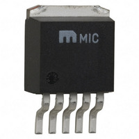
MIC2171WU Micrel Inc, MIC2171WU Datasheet - Page 7

MIC2171WU
Manufacturer Part Number
MIC2171WU
Description
IC REG SW 100KHZ 2.5A TO263-5
Manufacturer
Micrel Inc
Type
Step-Down (Buck), Step-Up (Boost), Inverting, Cukr
Datasheet
1.MIC2171WU_TR.pdf
(12 pages)
Specifications of MIC2171WU
Internal Switch(s)
Yes
Synchronous Rectifier
No
Number Of Outputs
1
Current - Output
2.5A
Frequency - Switching
100kHz
Voltage - Input
3 ~ 40 V
Operating Temperature
-40°C ~ 85°C
Mounting Type
Surface Mount
Package / Case
D²Pak, TO-263 (5 leads + tab)
Power - Output
1.3W
Number Of Pwm Outputs
1
On/off Pin
No
Adjustable Output
No
Switching Freq
112KHz
Operating Supply Voltage (max)
40V
Output Current
2.5A
Output Voltage
65V
Synchronous Pin
No
Operating Temperature Classification
Industrial
Mounting
Surface Mount
Pin Count
5 +Tab
Package Type
TO-263
Duty Cycle
95%
Lead Free Status / RoHS Status
Lead free / RoHS Compliant
Voltage - Output
-
Lead Free Status / RoHS Status
Compliant, Lead free / RoHS Compliant
Other names
576-1063
Available stocks
Company
Part Number
Manufacturer
Quantity
Price
Company:
Part Number:
MIC2171WU
Manufacturer:
MIC
Quantity:
740
The junction temperature for any semiconductor is
calculated using the following:
where:
For the practical example:
then:
This junction temperature is below the rated maximum of
150°C.
Grounding
Refer to Figure 5. Heavy lines indicate high current
paths.
A single point ground is strongly recommended for
proper operation.
The signal ground, compensation network ground, and
feed-back network connections are sensitive to minor
voltage variations. The input and output capacitor
grounds and power ground conductors will exhibit
voltage drop when carrying large currents. Keep the
sensitive circuit ground traces separate from the power
ground traces. Small voltage variations applied to the
sensitive circuits can prevent the MIC2171 or any
switching regulator from functioning properly.
Boost Conversion
Refer to Figure 1 for a typical boost conversion
application where a +5V logic supply is available but
+12V at 0.25A is required.
The first step in designing a boost converter is
determining whether inductor L1 will cause the converter
to operate in either continuous or discontinuous mode.
Micrel, Inc.
May 2007
V
IN
T
T
T
P
θ
T
θ
T
T
JA
JA
J
J
A
A
J
J
(total)
= T
= junction temperature
= 70 + (1.24 × 45)
= 126°C
= ambient temperature (maximum)
= 70°C
= junction to ambient thermal resistance
= 45°C/W (TO-220)
Figure 5. Single Point Ground
= total power dissipation
A
+ P
(total)
GND
MIC2171
θ
IN
JA
V C
S W
F B
Single point ground
7
Discontinuous mode is preferred because the feedback
control of the converter is simpler.
When L1 discharges its current completely during the
MIC2171 off-time, it is operating in discontinuous mode.
L1 is operating in continuous mode if it does not
discharge completely before the MIC2171 power switch
is turned on again.
Discontinuous Mode Design
Given the maximum output current, solve equation (1) to
determine
discontinuous mode without initiating the internal device
current limit.
(1)
(1a)
where:
For the example in Figure 1.
then:
This value is greater than the 0.25A output current
requirement, so we can proceed to find the minimum
inductance value of L1 for discontinuous operation at
P
(2)
OUT
.
I
I
V
δ = duty cycle
V
V
I
I
V
δ = 0.662
V
V
I
I
δ
I
L1
CL
OUT
OUT
CL
OUT
OUT
OUT
IN(min)
OUT
F
IN(min)
OUT
F
=
= D1 forward voltage drop
= 0.36V (@ .26A, 70°C)
= internal switch current limit
= 1.67 (2–0.662) = 2.24A
≥
= maximum output current
= 0.25A
≤ 0.258A
whether
V
= required output voltage
= 12.0V
≤
≤
2P
I
I
(Refer to Electrical Characteristics.)
OUT
(V
CL
CL
= minimum input voltage = V
= 4.18V
⎛
⎜ ⎜
⎝
⎛
⎜
⎝
OUT
I
IN
2.235
= 2.5A when δ < 50%
= 1.67 (2 – δ) when δ ≥ 50%
CL
V
2
δ
+
OUT
2
f
V
)
⎞
⎟ ⎟
⎠
V
SW
2
V
OUT
F
IN(min)
⎞
⎟
⎠
+
the
−
×
V
V
4.178
12
F
IN(min)
δ
device
×
0.662
can
M9999-051107
IN
operate
– V
MIC2171
SW
in


