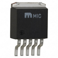
MIC2171WU Micrel Inc, MIC2171WU Datasheet - Page 8

MIC2171WU
Manufacturer Part Number
MIC2171WU
Description
IC REG SW 100KHZ 2.5A TO263-5
Manufacturer
Micrel Inc
Type
Step-Down (Buck), Step-Up (Boost), Inverting, Cukr
Datasheet
1.MIC2171WU_TR.pdf
(12 pages)
Specifications of MIC2171WU
Internal Switch(s)
Yes
Synchronous Rectifier
No
Number Of Outputs
1
Current - Output
2.5A
Frequency - Switching
100kHz
Voltage - Input
3 ~ 40 V
Operating Temperature
-40°C ~ 85°C
Mounting Type
Surface Mount
Package / Case
D²Pak, TO-263 (5 leads + tab)
Power - Output
1.3W
Number Of Pwm Outputs
1
On/off Pin
No
Adjustable Output
No
Switching Freq
112KHz
Operating Supply Voltage (max)
40V
Output Current
2.5A
Output Voltage
65V
Synchronous Pin
No
Operating Temperature Classification
Industrial
Mounting
Surface Mount
Pin Count
5 +Tab
Package Type
TO-263
Duty Cycle
95%
Lead Free Status / RoHS Status
Lead free / RoHS Compliant
Voltage - Output
-
Lead Free Status / RoHS Status
Compliant, Lead free / RoHS Compliant
Other names
576-1063
Available stocks
Company
Part Number
Manufacturer
Quantity
Price
Company:
Part Number:
MIC2171WU
Manufacturer:
MIC
Quantity:
740
where:
For our practical example:
Equation (3) solves for L1’s maximum current value.
(3)
where:
Use a 15µH inductor with a peak current rating of at
least 2A.
Flyback Conversion
Flyback converter topology may be used in low power
applications where voltage isolation is required or
whenever the input voltage can be less than or greater
than the output voltage. As with the step-up converter
the inductor (transformer primary) current can be
continuous or discontinuous. Discontinuous operation is
recommended.
Figure 2 shows a practical flyback converter design
using the MIC2171.
Switch Operation
During Q1’s on time (Q1 is the internal NPN transistor—
see block diagrams), energy is stored in T1’s primary
inductance. During Q1’s off time, stored energy is
partially discharged into C4 (output filter capacitor).
Careful selection of a low ESR capacitor for C4 may
provide satisfactory output ripple voltage making
additional filter stages unnecessary.
C1 (input capacitor) may be reduced or eliminated if the
MIC2171 is located near a low impedance voltage
source.
Output Diode
The output diode allows T1 to store energy in its primary
inductance (D2 non-conducting) and release energy into
C4 (D2 conducting). The low forward voltage drop of a
Schottky diode minimizes power loss in D2.
Frequency Compensation
A simple frequency compensation network consisting of
R3 and C2 prevents output oscillations.
High impedance output stages (transconductance type)
in the MIC2171 often permit simplified loop-stability
Micrel, Inc.
May 2007
P
f
L1 ≥ 12.4µH (use 15µH)
T
I
L1
I
I
SW
L1(peak)
L1(peak)
L1(peak)
ON
OUT
≥
= 1×10⁵Hz (100kHz)
= δ / fSW = 6.62×10⁻⁶ sec
= 12 × 0.25 = 3W
(
2
4.178
= 1.84A
×
=
=
3.0
4.178
V
IN
×
×
L1
T
0.662
1
ON
15
×
×
10
×
6.62
)
10
5
2
−
×
6
10
−
6
8
solutions to be connected to circuit ground, although a
more
components from the error amplifier output to its
inverting input is also possible.
Voltage Clipper
Care must be taken to minimize T1’s leakage
inductance,
incorporate the voltage clipper consisting of D1, R4, and
C3 to avoid second breakdown (failure) of the
MIC2171’s internal power switch.
Discontinuous Mode Design
When designing a discontinuous flyback converter, first
determine whether the device can safely handle the
peak primary current demand placed on it by the output
power. Equation (8) finds the maximum duty cycle
required for a given input voltage and output power. If
the duty cycle is greater than 0.8, discontinuous
operation cannot be used.
(8)
For a practical example let: (see Figure 2)
then:
A few iterations of equation (8) may be required if the
duty cycle is found to be greater than 50%.
Calculate the maximum transformer turns ratio a, or
N
MIC2171 power switch.
(9)
where:
PRI
/N
SEC
conventional
P
V
I
V
V
V
δ ≥ 0.74 (74%), less than 0.8 so discontinuous is
permitted.
a = transformer maximum turns ratio
V
voltage
F
commercial and industrial applications)
V
V
V
δ
a
CL
, that will guarantee safe operation of the
CE
OUT
IN
IN(min)
CE
IN(max)
SEC
F
IN(min)
IN(min)
≤
≥
)
= 2.5A when δ < 50%
= 4.0V to 6.0V
= power switch collector to emitter maximum
I
V
1.67 (2 – δ) when δ ≥ 50%
CL
= 5.0V × 0.5A = 2.5W
= safety derating factor (0.8 for most
= transformer secondary voltage (V
otherwise
CE
= V
= 4 – 0.78V
= 3.22V
= maximum input voltage
(
V
F
CE
IN(min)
IN
V
2P
SEC
– (I
−
OUT
V
technique
−
CL
IN(max)
VSW
it
× R
SW
may
)
of
be
connecting
M9999-051107
necessary
MIC2171
OUT
the
to
+


