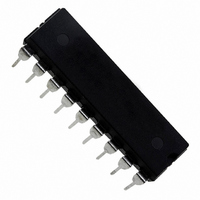
L4963W STMicroelectronics, L4963W Datasheet

L4963W
Specifications of L4963W
L4963W
Available stocks
Related parts for L4963W
L4963W Summary of contents
Page 1
... This is advanced information on a new product now in development or underogin evaluation. Details are subject to change without notice. 1.5A SWITCHING REGULATOR Powerdip12+3+3 ORDERING NUMBERS: L4963W The L4963 is mounted in a 12+3+3 lead Powerdip (L4963) and SO20 large (L4963D) plastic pack- ages and requires very few external components. ...
Page 2
L4963 - L4963D ABSOLUTE MAXIMUM RATINGS Symbol SO20 Powerdip – ...
Page 3
PIN FUNCTIONS SO20L Power DIP 14, 15, 16, 17 13, 14 ...
Page 4
L4963 - L4963D CIRCUIT DESCRIPTION (Refer to Block Dia- gram) The L4963 is a monolithic stepdown regulator pro- viding 1.5A at 5.1V working in discontinuous vari- able frequency mode. In normal operation the device resonates at a frequency depending primar- ...
Page 5
ELECTRICAL CHARACTERISTIC (Refer to the test circuit V Symbol Parameter DYNAMIC CHARACTERISTICS V Output Voltage Range o V Input Voltage Range i V Feedback Voltage 12 I Input Bias Current 12 V Input Offset Voltage OS12 V Line Regulation o ...
Page 6
L4963 - L4963D ELECTRICAL CHARACTERISTIC (Continued) Symbol Parameter RESET V Rising Threshold Voltage 12 V Falling Threshold Voltage 12 Delay Rising Thereshold V 9D Voltage Delay Falling Thereshold V 9F Voltage –I Delay Source Current 9SO I Delay Sink Current ...
Page 7
Figure 2: Test Circuit Figure 3: DC Test Circuit Figure 3a Figure 3b L4963 - L4963D 7/17 ...
Page 8
L4963 - L4963D Figure 3c Figure 4: Quiescent Drain Current vs. Supply Voltage (0% Duty Cycle) Figure 6: Quiescent Drain Current vs. Junction Temperature (0% Duty Cycle) 8/17 Figure 5: Quiescent Drain Current vs. Supply Voltage (100% Duty Cycle) Figure ...
Page 9
Figure 8: Reference Voltage vs. V Figure 10: Line Transient Response Figure 12: Supply Voltage Ripple Rejection vs. Frequency Figure 9: Reference Voltage vs Figure 11: Load Transient Figure 13: Dropout Voltage Between pi3 and 2 L4963 - ...
Page 10
L4963 - L4963D Figure 14: Dropout Voltage Between pin3 and 2 vs. Junction Temperature Figure 16: Power Dissipation (device only) vs. In- put Voltage (Powerdip Package Only) Figure 18: Voltage and Current Waveform at pin2 10/17 Figure 15: Maximum Allowable ...
Page 11
Figure 20: Efficiency vs. Output Voltage (Power- dip Package Only) Figure 22: Current Limit vs. Input Voltage Figure 24: Oscillator Frequency vs. Junction Temperature Figure 21: Current Limit vs. Junction Tempera- ture V = 30V i Figure 23: Oscillator Frequency ...
Page 12
L4963 - L4963D Figure 26: Evaluation Board Circuit PART LIST CAPACITOR C1 1000 F 50V EKR (*) C2 2.2mF 16V C3 1000 F 40V with low ESR 50V film RESISTOR 51K ...
Page 13
Figure 27: P.C. Board and Component Layout of the Circuit of fig. 26 (Powerdip Package) (1:1 scale). Figure 28: Thermal Characteristics Figure 29: Junction to Ambient Thermal Resis- tance vs. Area on Board Heatsink (SO20) L4963 - L4963D 13/17 ...
Page 14
L4963 - L4963D Figure 30: A Minimal 5.1 Fixed Regulator — Very Few Components are Required Figure 31: A Minimal Components count for V 14/17 = 12V O ...
Page 15
DIM. MIN. TYP. MAX. MIN. a1 0.51 0.020 B 0.85 1.40 0.033 b 0.50 b1 0.38 0.50 0.015 D 24.80 E 8.80 e 2.54 e3 20.32 F 7.10 I 5.10 L 3.30 Z 2.54 inch MECHANICAL DATA TYP. MAX. ...
Page 16
L4963 - L4963D mm DIM. MIN. TYP. MAX. A 2.35 2.65 0.093 A1 0.1 0.3 0.004 B 0.33 0.51 0.013 C 0.23 0.32 0.009 D 12.6 13 0.496 E 7.4 7.6 0.291 e 1. 10.65 0.394 h 0.25 ...
Page 17
... No license is granted by implication or otherwise under any patent or patent rights of STMicroelectronics. Specification mentioned in this publication are subject to change without notice. This publication supersedes and replaces all information previously supplied. STMicroelectronics products are not authorized for use as critical components in life support devices or systems without express written approval of STMicroelectronics ...


