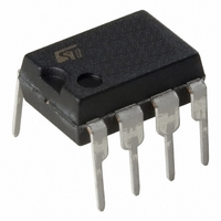
L4971 STMicroelectronics, L4971 Datasheet

L4971
Specifications of L4971
E-L4971
E-L4971
L4971
Available stocks
Related parts for L4971
L4971 Summary of contents
Page 1
... SOFT START FUNCTION ■ 2 DESCRIPTION The L4971 is a step down monolithic power switching regulator delivering 1. voltage be- tween 3.3V and 50V (selected by a simple external divider). Realized in BCD mixed technology, the device uses an internal power D-MOS transistor (with a typical Rdson of 0.25Ω) to obtain very high efficency and high switching speed ...
Page 2
... L4971 Figure 2. Block Diagram THERMAL SHUTDOWN 2 SS_INH INHIBIT 7 COMP 8 E/A FB 3.3V OSCILLATOR 3 OSC Figure 3. Pin Connections GND 1 SS_INH 2 OSC 3 OUT 4 D97IN595 DIP8 Table 2. Pin Description DIP SO (*) Name 1 2 GND Ground 2 3 SS_INH A logic signal (active low) disables the device (sleep mode operation). ...
Page 3
... Vcc = 8 to 55V 125°C Value int. limit -0.3 DIP8 1 SO16 0.8 -40 to 150 DIP8 SO16 Max. 90 (*) 110 (*) Min. Typ. Max 3.33 3.36 3.39 3.292 3.36 3.427 * 3.22 3.36 3.5 0.44 0. 100 110 L4971 Unit °C Unit °C/W Unit KHz 3/13 ...
Page 4
... L4971 Table 25°C, Cosc = 2.7nF, Rosc = 20kΩ Specification Refered to T Soft Start Soft start charge current Soft start discharge current Inhibit V Low level voltage LL I Isource Low level sLL DC Characteristics I Total operating quiescent qop current I Quiescent current q I Total stand-by quiescent ...
Page 5
... C 4 22nF Load Regulation V =35V 55V CC CC 3mV 3mV =15 to 55V =3.3V/1. 126µH R (77120 330µF PS3L60U R 4 D97IN749A L4971 V (V) R3(KΩ) R4(KΩ) O 3.3 0 5.1 2 4.7 L4971 = 0.5 to 1.5A O 6mV 6mV 4mV 5/13 ...
Page 6
... L4971 Figure 6. Quiescent drain current vs. input voltage. Iq (mA) 200KHz R =22K 1 C =1.2nF Tamb=25˚ Figure 7. Quiescent current vs. junction temperature Iq (mA 100KHz =35V -50 -30 - 110 Figure 8. Stand-by drain current vs. input voltage Ibias (µA) Vss=GND 150 Tj=25˚C 140 130 120 110 100 ...
Page 7
... =1. η (%) V = =12V =24V =48V 75 CC fsw=100KHz 70 V =5. 0.0 0.2 0.4 0.6 0.8 1.0 1.2 1.4 I η (%) V = =12V CC V =24V =48V fsw=100KHz V =3.36V 0.2 0.4 0.6 0.8 1.0 1.2 1.4 I L4971 D97IN737 =35V 25 V (V) O D97IN738 (A) O D97IN739 (A) O 7/13 ...
Page 8
... L4971 Figure 18. Efficiency vs. output current. η (%) 90 V =12V CC V =24V =48V 0.2 0.4 0.6 0.8 1.0 1.2 1.4 I Figure 19. Efficiency vs. output current. η (%) V = =12V =24V =48V 0.0 0.2 0.4 0.6 0.8 1.0 1.2 1.4 I Figure 20. Efficiency vs η (%) =1. 8/13 Figure 21. Power dissipation vs. Vcc. ...
Page 9
... D97IN786 V O (mV 100 = 100KHz 0 -100 D97IN745 470nF 330nF 220nF 100nF (V) CCmax Inductor and Vccmax L (µH) fsw=200KHz 300 200 100 error amplifier GAIN D97IN787 (dB) 50 GAIN 0 -50 -100 Phase -150 -200 L4971 D97IN746 56nF 47nF 33nF 22nF max(V) CC Phase 135 8 f(Hz) 9/13 ...
Page 10
... L4971 Figure 29. DIP8 Mechanical Data & Package Dimensions mm DIM. MIN. TYP. MAX. A 3.32 a1 0.51 B 1.15 1.65 b 0.356 0.55 b1 0.204 0.304 D 10.92 E 7.95 9.75 e 2.54 e3 7.62 e4 7.62 F 6.6 I 5.08 L 3.18 3.81 Z 1.52 10/13 inch MIN. TYP. MAX. 0.131 0.020 0.045 0.065 0.014 ...
Page 11
... Mold flash, protusions or gate burrs shall not exceed 0.15mm per side. inch MIN. TYP. MAX. 0.093 0.104 0.004 0.012 0.013 0.200 0.009 0.013 0.398 0.413 0.291 0.299 0.050 0.394 0.419 0.010 0.030 0.016 0.050 0.004 OUTLINE AND MECHANICAL DATA SO16 (Wide) 0016021 C L4971 11/13 ...
Page 12
... L4971 4 REVISION HISTORY Table 7. Revision History Date Revision October 2004 May 2005 12/13 10 First Issue in EDOCS 11 Updated the Layout look & feel. Changed name of the D1 on the figs. 1 and 4. Description of Changes ...
Page 13
... Australia - Belgium - Brazil - Canada - China - Czech Republic - Finland - France - Germany - Hong Kong - India - Israel - Italy - Japan - Malaysia - Malta - Morocco - Singapore - Spain - Sweden - Switzerland - United Kingdom - United States of America All other names are the property of their respective owners © 2005 STMicroelectronics - All rights reserved STMicroelectronics group of companies www.st.com L4971 13/13 ...


