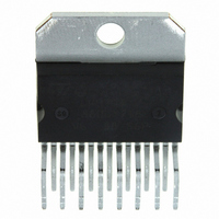
L4970A STMicroelectronics, L4970A Datasheet

L4970A
Specifications of L4970A
Available stocks
Related parts for L4970A
L4970A Summary of contents
Page 1
... Realized with BCD mixed technology, the device uses a DMOS output transistor to obtain very high efficiency and very fast switching times. Features of the L4970A include reset and power fail for mi- croprocessors, feed forward line regulation, soft start, limiting current and thermal protection. The ...
Page 2
... L4970A ABSOLUTE MAXIMUM RATINGS Symbol V Input Voltage 9 V Input Operating Voltage 9 V Output DC Voltage 7 Output Peak Voltage 0 200KHz I Maximum Output Current 7 V Bootstrap Voltage 6 Bootstrap Operating Voltage Input Voltage at Pins Reset Output Voltage 4 I Reset Output Sink Current Input Voltage at Pin 5, 10, 11, 13 ...
Page 3
... It is connected via a divider for higher voltages. Soft Start Time Constant. A capacitor is connected between thi sterminal and ground to define the soft start time constant. Multiple L4970A are synchronized by connecting pin 13 inputs together or via an external syncr. pulse. 5.1V V Device Reference Voltage. ...
Page 4
... L4970A Figure 1: Feedforward Waveform Figure 2: Soft Start Function Figure 3: Limiting Current Function 4/21 ...
Page 5
... Fig 4B shows the case when the output is 5.1V but the supply voltage is not yet higher than the fixed threshold. The thermal protection disables circuit operation when the junction temperature reaches about 150 C and has an hysterysis to prevent unstable conditions. L4970A 5/21 ...
Page 6
... L4970A ELECTRICAL CHARACTERISTICS (Refer to the test circuit 2.2nF 200KHz typ, unless otherwise specified DYNAMIC CHARACTERISTICS Symbol Parameter V input Voltage Range (pin Output Votage o V Line Regulation o V Load Regulation o V Dropout Voltage Between d Pin 9 and 7 I Max. Limiting Current 7L Efficiency SVR Supply Voltage Ripple Reject ...
Page 7
... Test Condition Min 1 15V 45V 100 1mA 2.4 Test Condition Min 15V to 50V –0 3 0.9V 3.5V 2.5V 0.3 thr L4970A Typ. Max. Unit Fig Typ. Max. Unit Fig. 100 130 0 Typ. Max. Unit Fig 1 150 A 7C 150 – ...
Page 8
... L4970A ELECTRICAL CHARACTERISTICS (continued) RESET AND POWER FAIL FUNCTIONS Symbol Parameter V Rising Threshold Voltage 11R (pin 11) V Falling Threshold Voltage 11F (pin 11) V Delay High Threshold 5H Voltage V Delay Low Threshold 5L Voltage –I Delay Source Current 5SO I Delay Sink Current 5SI V Out Saturation Voltage ...
Page 9
... ESR Table A EYF (ROE L Table B = 220 F 40V EKR L SUGGESTED BOOTSTRAP CAPACITORS Operating Frequency 12V 4.7k 15V 4.7k 18V 4.7k 24V 4.7k Bootstrap Cap.c10 f = 20KHz 680nF f = 50KHz 470nF f = 100KHz 330nF f = 200KHz 220nF f = 500KHz 100nF L4970A R 7 6.2kW 9.1k 12k 18k 9/21 ...
Page 10
... L4970A Figure 6b: P.C. Board (Back side) and Components Layout of the Circuit of Fig. 5. (1:1 scale) Figure 7: DC Test Circuits 10/21 ...
Page 11
... Figure 7A Figure 7B L4970A 11/21 ...
Page 12
... L4970A Figure 7D Figure 7C 12/21 ...
Page 13
... Voltage (0% duty cycle - see fig. 7A). Figure 10: Quiescent Drain Current vs. Duty Cycle Figure 12: Reference Voltage (pin 14) vs. Junction Temperature (see fig. 7) Figure 9: Quiescent Drain Current vs. Junction Temperature (0% duty cycle). Figure 11: Reference Voltage (pin14) vs. V fig. 7) Figure 13: Reference Voltage (pin15) vs. V fig. 7) L4970A (see i (see i 13/21 ...
Page 14
... L4970A Figure 14: Reference Voltage (pin 15) vs. Junction Temperature (see fig. 7) Figure 16: Switching Frequency vs. Input Voltage (see fig. 5) Figure 18: Switching Frequency vs. R4 (see fig. 5) 14/21 Figure 15: Reference Voltage 5.1V (pin 14) Supply Voltage Ripple Rejection vs. Frequency Figure 17: Switching Frequency vs. Junction Temperature (see fig 5) ...
Page 15
... Figure 22: Load Transient Response (see fig. 5) Figure 24: Dropout Voltage Between Pin 9 and Pin 7 vs. Junction Temperature Figure 21: Line Transient Response (see fig. 5) Figure 23: Dropout Voltage Between Pin 9 and Pin 7 vs. Current at Pin 7 Figure 25: Power Dissipation (device only) vs. Input Voltage L4970A 15/21 ...
Page 16
... L4970A Figure 26: Power Dissipation (device only) vs. Output Voltage Figure 28: Efficiency vs. Output Current Figure 30: Efficiency vs. Output Voltage 16/21 Figure 27: Heatsink Used to Derive the Device’s Power Dissipation T case R - Heatsink = th Figure 29: Efficiency vs. Output Voltage Figure 31: Open Loop Frequency and Phase Response of Error Amplifier (see fig ...
Page 17
... Figure 32: Power Dissipation Derating Curve Figure 33: A5.1V/12V Multiple Supply. Note the Synchronization between the L4970A and the L4974A L4970A 17/21 ...
Page 18
... L4970A Figure 34: 5.1V / 10A Low Cost Application Figure 35: 10A Switching Regulator, Adjustable from 0V to 25V. 18/21 ...
Page 19
... Figure 36: L4970A’s Sync. Example L4970A 19/21 ...
Page 20
... L4970A mm DIM. MIN. TYP. MAX 2. 0.49 0.55 0.019 F 0.66 0.75 0.026 G 1.02 1.27 1.52 0.040 G1 17.53 17.78 18.03 0.690 H1 19.6 0.772 H2 20.2 L 21.9 22.2 22.5 0.862 L1 21.7 22.1 22.5 0.854 L2 17.65 18.1 0.695 L3 17.25 17.5 17.75 0.679 L4 10.3 10.7 10 ...
Page 21
... STMicroelectronics – Printed in Italy – All Rights Reserved Australia - Brazil - China - Finland - France - Germany - Hong Kong - India - Italy - Japan - Malaysia - Malta - Morocco - Singapore - Spain - Sweden - Switzerland - United Kingdom - U.S.A. The ST logo is a registered trademark of STMicroelectronics STMicroelectronics GROUP OF COMPANIES http://www.st.com L4970A 21/21 ...


