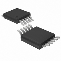
LTC3700EMS Linear Technology, LTC3700EMS Datasheet - Page 12

LTC3700EMS
Manufacturer Part Number
LTC3700EMS
Description
IC DC/DC CNTRLR STPDN LDO 10MSOP
Manufacturer
Linear Technology
Type
Step-Down (Buck)r
Datasheet
1.LTC3700EMS.pdf
(16 pages)
Specifications of LTC3700EMS
Topology
Step-Down (Buck) (1), Linear (LDO) (1)
Function
Any Function
Number Of Outputs
2
Frequency - Switching
550kHz
Voltage/current - Output 1
Adj to 0.8V, 5A
Voltage/current - Output 2
Adj to 0.8V, 150mA
W/led Driver
No
W/supervisor
No
W/sequencer
No
Voltage - Supply
2.4 V ~ 9.8 V
Operating Temperature
-40°C ~ 85°C
Mounting Type
Surface Mount
Package / Case
10-MSOP, Micro10™, 10-uMAX, 10-uSOP
Current - Output
1A
Voltage - Output
0.8 ~ 5 V
Voltage - Input
2.65 ~ 9.8 V
Internal Switch(s)
No
Synchronous Rectifier
No
Lead Free Status / RoHS Status
Contains lead / RoHS non-compliant
Power - Output
-
Available stocks
Company
Part Number
Manufacturer
Quantity
Price
Company:
Part Number:
LTC3700EMS
Manufacturer:
Linear Technology
Quantity:
135
Company:
Part Number:
LTC3700EMS
Manufacturer:
LT
Quantity:
10 000
Part Number:
LTC3700EMS
Manufacturer:
LINEAR/凌特
Quantity:
20 000
LTC3700
APPLICATIONS
In applications where the maximum duty cycle is less than
100% and the buck is in continuous mode, the R
governed by:
where DC is the maximum operating duty cycle of the
buck.
Output Diode Selection
The catch diode carries load current during the off-time.
The average diode current is therefore dependent on the
P-channel switch duty cycle. At high input voltages the
diode conducts most of the time. As V
the diode conducts only a small fraction of the time. The
most stressful condition for the diode is when the output
is short-circuited. Under this condition the diode must
safely handle I
it is important to adequately specify the diode peak current
and average power dissipation so as not to exceed the
diode ratings.
Under normal load conditions, the average current con-
ducted by the diode is:
The allowable forward voltage drop in the diode is calcu-
lated from the maximum short-circuit current as:
12
R
I
V
D
F
DS ON
(
I
V
SC MAX
IN
V
)
IN
P
(
D
PEAK
V
DC I
OUT
V
)
D
at close to 100% duty cycle. Therefore,
U
OUT
I
P
OUT
P
2
INFORMATION
1
U
p
W
IN
approaches V
U
DS(ON)
OUT
is
where P
determined by efficiency and/or thermal requirements.
A fast switching diode must also be used to optimize
efficiency. Schottky diodes are a good choice for low
forward drop and fast switching times. Remember to keep
lead length short and observe proper grounding (see
Board Layout Checklist) to avoid ringing and increased
dissipation.
C
In continuous mode, the source current of the P-channel
MOSFET is a square wave of duty cycle (V
(V
input capacitor sized for the maximum RMS current must
be used. The maximum RMS capacitor current is given by:
This formula has a maximum value at V
I
monly used for design because even significant deviations
do not offer much relief. Note that capacitor manufacturer’s
ripple current ratings are often based on 2000 hours of life.
This makes it advisable to further derate the capacitor, or
to choose a capacitor rated at a higher temperature than
required. Several capacitors may be paralleled to meet the
size or height requirements in the design. Due to the high
operating frequency of the LTC3700, ceramic capacitors
can also be used for C
if there is any question.
RMS
IN
IN
C
and C
+ V
IN
= I
Required
D
OUT
D
). To prevent large voltage transients, a low ESR
OUT
is the allowable power dissipation and will be
/2. This simple worst-case condition is com-
Selection
I
RMS
IN
. Always consult the manufacturer
I
MAX
V
OUT
V
IN
IN
V
IN
= 2V
V
OUT
OUT
OUT
, where
1 2 /
+ V
3700f
D
)/


