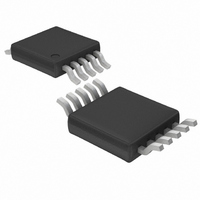
LTC3700EMS Linear Technology, LTC3700EMS Datasheet - Page 6

LTC3700EMS
Manufacturer Part Number
LTC3700EMS
Description
IC DC/DC CNTRLR STPDN LDO 10MSOP
Manufacturer
Linear Technology
Type
Step-Down (Buck)r
Datasheet
1.LTC3700EMS.pdf
(16 pages)
Specifications of LTC3700EMS
Topology
Step-Down (Buck) (1), Linear (LDO) (1)
Function
Any Function
Number Of Outputs
2
Frequency - Switching
550kHz
Voltage/current - Output 1
Adj to 0.8V, 5A
Voltage/current - Output 2
Adj to 0.8V, 150mA
W/led Driver
No
W/supervisor
No
W/sequencer
No
Voltage - Supply
2.4 V ~ 9.8 V
Operating Temperature
-40°C ~ 85°C
Mounting Type
Surface Mount
Package / Case
10-MSOP, Micro10™, 10-uMAX, 10-uSOP
Current - Output
1A
Voltage - Output
0.8 ~ 5 V
Voltage - Input
2.65 ~ 9.8 V
Internal Switch(s)
No
Synchronous Rectifier
No
Lead Free Status / RoHS Status
Contains lead / RoHS non-compliant
Power - Output
-
Available stocks
Company
Part Number
Manufacturer
Quantity
Price
Company:
Part Number:
LTC3700EMS
Manufacturer:
Linear Technology
Quantity:
135
Company:
Part Number:
LTC3700EMS
Manufacturer:
LT
Quantity:
10 000
Part Number:
LTC3700EMS
Manufacturer:
LINEAR/凌特
Quantity:
20 000
LTC3700
V
decoupled to GND (Pin 5).
LDO (Pin 2): LDO Output Pin. Must be closely decoupled
to GND (Pin 5) with a low ESR ceramic capacitor 2.2 F.
V
back voltage from an external resistor divider between
LDO (Pin 2) and GND (Pin 5).
PGOOD (Pin 4): Open-Drain Power Good Output. This pin
will pull to ground if either voltage output of the buck or the
LDO [sensed at V
is out of range. When both voltage outputs are valid, this
pin will go to a high impedance state.
GND (Pin 5): Common Ground Pin for Both Buck and LDO.
PGATE (Pin 6): Gate Drive for Buck’s External P-Channel
MOSFET. This pin swings from 0V to V
PIN
6
IN2
FB2
U
(Pin 1): LDO Input Supply Pin. Must be closely
(Pin 3): LDO Feedback Voltage. Receives the feed-
FUNCTIONS
U
FB
(Pin 9) and V
U
FB2
(Pin 3), respectively]
IN
.
V
decoupled to GND (Pin 5).
SENSE
parator of the Buck. Monitors switch current of external
P-Channel MOSFET.
V
back voltage from an external resistor divider between
buck output and GND (Pin 5).
I
serves as the error amplifier compensation point for the
buck, as well as a common run control input for both the
buck and the LDO. The current comparator threshold of
the buck increases with this voltage. Nominal voltage
range for this pin is 0.7V to 1.9V. Forcing this pin below
0.3V causes both the buck and the LDO to be shut down.
In shutdown all functions are disabled, the PGATE pin is
held high and the LDO output will go to a high impedance
state.
TH
IN
FB
/RUN (Pin 10): This pin performs two functions. It
(Pin 9): Buck Feedback Voltage. Receives the feed-
(Pin 7): Buck Input Supply Pin. Must be closely
–
(Pin 8): The Negative Input to the Current Com-
3700f


