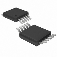
LTC3700EMS Linear Technology, LTC3700EMS Datasheet - Page 9

LTC3700EMS
Manufacturer Part Number
LTC3700EMS
Description
IC DC/DC CNTRLR STPDN LDO 10MSOP
Manufacturer
Linear Technology
Type
Step-Down (Buck)r
Datasheet
1.LTC3700EMS.pdf
(16 pages)
Specifications of LTC3700EMS
Topology
Step-Down (Buck) (1), Linear (LDO) (1)
Function
Any Function
Number Of Outputs
2
Frequency - Switching
550kHz
Voltage/current - Output 1
Adj to 0.8V, 5A
Voltage/current - Output 2
Adj to 0.8V, 150mA
W/led Driver
No
W/supervisor
No
W/sequencer
No
Voltage - Supply
2.4 V ~ 9.8 V
Operating Temperature
-40°C ~ 85°C
Mounting Type
Surface Mount
Package / Case
10-MSOP, Micro10™, 10-uMAX, 10-uSOP
Current - Output
1A
Voltage - Output
0.8 ~ 5 V
Voltage - Input
2.65 ~ 9.8 V
Internal Switch(s)
No
Synchronous Rectifier
No
Lead Free Status / RoHS Status
Contains lead / RoHS non-compliant
Power - Output
-
Available stocks
Company
Part Number
Manufacturer
Quantity
Price
Company:
Part Number:
LTC3700EMS
Manufacturer:
Linear Technology
Quantity:
135
Company:
Part Number:
LTC3700EMS
Manufacturer:
LT
Quantity:
10 000
Part Number:
LTC3700EMS
Manufacturer:
LINEAR/凌特
Quantity:
20 000
OPERATIO
when the buck is operating below 40% duty cycle. How-
ever, once the duty cycle exceeds 40%, slope com-
pensation begins and effectively reduces the peak induc-
tor current. The amount of reduction is given by the curves
in Figure 2.
Soft-Start
An internal default soft-start circuit is employed at power
up and/or when coming out of shutdown. The soft-start
circuit works by internally clamping the voltage at the I
RUN pin to the corresponding zero-current level and
gradually raising the clamp voltage such that the minimum
time required for the programmed switch current to reach
its maximum is approximately 0.5msec. After the soft-
start circuit has timed out, it is disabled until the part is put
in shutdown again or the input supply is cycled.
LDO Regulator
The 150mA low dropout (LDO) regulator on the LTC3700
employs an internal P-channel MOSFET pass device be-
tween its input supply (V
pass FET has an on-resistance of approximately 1.5
(with V
supply voltage. The dropout voltage is simply the FET on-
resistance multiplied by the load current when in dropout.
IN2
= 4.2V) with a strong dependence on input
U
(Refer to Functional Diagram)
IN2
) and the LDO output pin. The
Figure 2. Maximum Output Current vs Duty Cycle
110
100
90
80
70
60
50
40
30
20
10
0
10 20 30 40 50 60 70 80 90 100
I
AT 5% DUTY CYCLE
I
AT 5% DUTY CYCLE
V
RIPPLE
RIPPLE
IN
TH
= 4.2V
/
DUTY CYCLE (%)
= 0.4I
= 0.2I
PK
PK
The LDO is protected by both current limit and thermal
shutdown circuits. Current limit is set such that the output
voltage will start dropping out when the load current reaches
approximately 200mA. With a short-circuited LDO output,
the device will limit the sourced current to approximately
225mA. The thermal shutdown circuit has a typical trip
point of 150 C with a typical hysteresis of 5 C. In thermal
shutdown, the LDO pass device is turned off.
Frequency compensation of the LDO is accomplished by
forcing the dominant pole at the output. For stability, a low
ESR ceramic capacitor 2.2 F is required from LDO to
GND. For improved transient response, particularly at
heavy loads, it is recommended to use the largest value of
capacitor available in the same size considered.
Both the buck and the LDO share the same internally
generated bandgap reference voltage for their feedback
reference. When both input supplies are present, the
internal reference is powered by the buck input supply
(V
specified both with respect to V
present and with respect only to V
disabled. The same is true for V
will be higher when the buck is disabled by the current
draw of the internal reference.
IN
). For this reason, line regulation for the LDO output is
3700 F02
IN2
IN
and V
supply current, which
IN2
IN2
LTC3700
if the buck is
if the buck is
9
3700f


