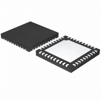
MAX15035ETL+ Maxim Integrated Products, MAX15035ETL+ Datasheet - Page 13

MAX15035ETL+
Manufacturer Part Number
MAX15035ETL+
Description
IC REG STEP DOWN 15A 40-TQFN
Manufacturer
Maxim Integrated Products
Type
Step-Down (Buck)r
Datasheet
1.MAX15035ETL.pdf
(26 pages)
Specifications of MAX15035ETL+
Internal Switch(s)
Yes
Synchronous Rectifier
Yes
Number Of Outputs
1
Voltage - Output
1.05V, 1.5V
Current - Output
15A
Voltage - Input
4.5 ~ 26 V
Operating Temperature
-40°C ~ 85°C
Mounting Type
Surface Mount
Package / Case
40-TQFN Exposed Pad
Power - Output
2.16W
Lead Free Status / RoHS Status
Lead free / RoHS Compliant
Frequency - Switching
-
Lead Free Status / Rohs Status
Lead free / RoHS Compliant
The MAX15035 standard application circuit (Figure 1)
generates a 1.5V or 1.05V output rail for general-purpose
use. See Table 1 for component selections. Table 2 lists
the component suppliers.
The MAX15035 step-down controller is ideal for low-
duty-cycle (high-input voltage to low-output voltage)
applications. Maxim’s proprietary Quick-PWM pulse-
width modulator in the MAX15035 is specifically
designed for handling fast-load steps while maintaining
a relatively constant operating frequency and inductor
operating point over a wide range of input voltages.
The Quick-PWM architecture circumvents the poor
load-transient timing problems of fixed-frequency, cur-
rent-mode PWMs while also avoiding the problems
caused by widely varying switching frequencies in con-
ventional constant-on-time (regardless of input voltage)
pulse-frequency modulation (PFM) control schemes.
The MAX15035 requires an external 5V bias supply in
addition to the input. See Figure 6 for an optional 5V
bias generation circuit.
The 5V bias supply powers both the PWM controller
and internal gate-drive power, so the maximum current
drawn is determined by:
The MAX15035 includes a 20Ω resistor between V
and V
The Quick-PWM control architecture is a pseudo-fixed-
frequency, constant on-time, current-mode regulator
with voltage feed-forward (Figure 2). This architecture
relies on the output filter capacitor’s ESR to act as a
current-sense resistor, so the output ripple voltage pro-
vides the PWM ramp signal. The control algorithm is
simple: the high-side switch on-time is determined sole-
ly by a one-shot whose pulse width is inversely propor-
tional to input voltage and directly proportional to
output voltage. Another one-shot sets a minimum off-
time (200ns typ). The on-time one-shot is triggered if
the error comparator is low, the low-side switch current
is below the valley current-limit threshold, and the mini-
mum off-time one-shot has timed out.
15A Step-Down Regulator with Internal Switches
CC
Free-Running Constant-On-Time PWM
I
BIAS
, simplifying the PCB layout requirement.
Standard Application Circuit
Controller with Input Feed-Forward
= I
Q
+ f
______________________________________________________________________________________
SW
+5V Bias Supply (V
Detailed Description
Q
G
= 2mA to 20mA (typ)
CC
/V
DD
DD
)
The heart of the PWM core is the one-shot that sets the
high-side switch on-time. This fast, low-jitter, adjustable
one-shot includes circuitry that varies the on-time in
response to input and output voltage. The high-side
switch on-time is inversely proportional to the input volt-
age as sensed by the TON input, and proportional to
the feedback voltage as sensed by the FB input:
where t
(R
a nearly constant switching frequency despite the lack
of a fixed-frequency clock generator. Connect a resis-
tor (R
period t
where C
back (V
to switching periods of 167ns (600kHz) to 500ns
(200kHz), respectively. High-frequency (600kHz) opera-
tion optimizes the application for the smallest compo-
nent size, trading off efficiency due to higher switching
losses. This may be acceptable in ultra-portable devices
where the load currents are lower and the controller is
powered from a lower voltage supply. Low-frequency
(200kHz) operation offers the best overall efficiency at
the expense of component size and board space.
For continuous conduction operation, the actual switching
frequency can be estimated by:
where V
the inductor discharge path, including synchronous recti-
fier, inductor, and PCB resistances; V
the resistances in the charging path, including the high-
side switch, inductor, and PCB resistances; and t
the on-time calculated by the MAX15035.
The MAX15035 is enabled when EN is driven high and
the 5V bias supply (V
powers up first. Once the reference exceeds its UVLO
threshold, the internal analog blocks are turned on and
masked by a 50μs one-shot delay in order to allow the
bias circuitry and analog blocks enough time to settle
to their proper states. With the control circuitry reliably
powered up, the PWM controller may begin switching.
TON
TON
) between TON and V
OUT
SW
SW
TON
DIS
) between TON and V
t
SW
= 1/f
(switching period) is set by the resistance
= V
is the sum of the parasitic voltage drops in
Power-Up Sequence (POR, UVLO)
On-Time (t
= 16.26pF. When used with unity-gain feed-
=
FB
SW
C
f
SW
TON
), a 96.75kΩ to 303.25kΩ corresponds
:
=
(
t
R
ON
ON IN
DD
TON
V
) = t
(
) is present. The reference
FB
V
IN
+
+
SW
. This algorithm results in
6 5 . Ω
−
V
DIS
V
IN
CHG
(V
k
to set the switching
On-Time One-Shot
FB
)
CHG
⎛
⎝ ⎜
)
/V
V
V
OUT
IN
FB
)
is the sum of
⎞
⎠ ⎟
ON
13
is


