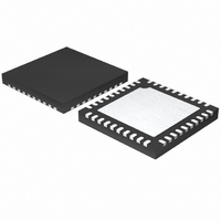
MAX15035ETL+ Maxim Integrated Products, MAX15035ETL+ Datasheet - Page 24

MAX15035ETL+
Manufacturer Part Number
MAX15035ETL+
Description
IC REG STEP DOWN 15A 40-TQFN
Manufacturer
Maxim Integrated Products
Type
Step-Down (Buck)r
Datasheet
1.MAX15035ETL.pdf
(26 pages)
Specifications of MAX15035ETL+
Internal Switch(s)
Yes
Synchronous Rectifier
Yes
Number Of Outputs
1
Voltage - Output
1.05V, 1.5V
Current - Output
15A
Voltage - Input
4.5 ~ 26 V
Operating Temperature
-40°C ~ 85°C
Mounting Type
Surface Mount
Package / Case
40-TQFN Exposed Pad
Power - Output
2.16W
Lead Free Status / RoHS Status
Lead free / RoHS Compliant
Frequency - Switching
-
Lead Free Status / Rohs Status
Lead free / RoHS Compliant
15A Step-Down Regulator with Internal Switches
When only using ceramic output capacitors, output
overshoot (V
output capacitance requirement. Their relatively low
capacitance value may allow significant output over-
shoot when stepping from full-load to no-load condi-
tions, unless designed with a small inductance value
and high switching frequency to minimize the energy
transferred from the inductor to the capacitor during
load-step recovery.
Unstable operation manifests itself in two related but
distinctly different ways: double pulsing and feedback-
loop instability. Double pulsing occurs due to noise on
the output or because the ESR is so low that there is
not enough voltage ramp in the output voltage signal.
This “fools” the error comparator into triggering a new
cycle immediately after the minimum off-time period
has expired. Double pulsing is more annoying than
harmful, resulting in nothing worse than increased out-
put ripple. However, it can indicate the possible pres-
ence of loop instability due to insufficient ESR. Loop
instability can result in oscillations at the output after
line or load steps. Such perturbations are usually
damped, but can cause the output voltage to rise
above or fall below the tolerance limits.
The easiest method for checking stability is to apply a
very fast zero-to-max load transient and carefully
observe the output voltage-ripple envelope for over-
shoot and ringing. It can help to simultaneously monitor
the inductor current with an AC current probe. Do not
allow more than one cycle of ringing after the initial
step-response under/overshoot.
The input capacitor must meet the ripple current
requirement (I
The I
lowing equation:
The worst-case RMS current requirement occurs when
operating with V
equation simplifies to I
For most applications, nontantalum chemistries (ceramic,
aluminum, or OS-CON) are preferred due to their resis-
tance to inrush surge currents typical of systems with a
mechanical switch or connector in series with the input.
If the Quick-PWM controller is operated as the second
stage of a two-stage power-conversion system, tanta-
lum input capacitors are acceptable. In either configu-
ration, choose an input capacitor that exhibits less than
+10°C temperature rise at the RMS input current for
optimal circuit longevity.
24
______________________________________________________________________________________
RMS
requirements may be determined by the fol-
I
RMS
SOAR
RMS
=
IN
⎛
⎜
⎝
) imposed by the switching currents.
) typically determines the minimum
I
LOAD
= 2V
V
IN
RMS
Input Capacitor Selection
⎞
⎟
⎠
OUT
= 0.5 x I
V
OUT IN
. At this point, the above
(
V
LOAD
−
V
OUT
.
)
The output voltage-adjustable range for continuous-
conduction operation is restricted by the nonadjustable
minimum off-time one-shot. For best dropout perfor-
mance, use the slower (200kHz) on-time settings. When
working with low-input voltages, the duty-factor limit
must be calculated using worst-case values for on- and
off-times. Manufacturing tolerances and internal propa-
gation delays introduce an error to the on-times. This
error is greater at higher frequencies. Also, keep in
mind that transient response performance of buck reg-
ulators operated too close to dropout is poor, and bulk
output capacitance must often be added (see the V
equation in the Quick-PWM Design Procedure section).
The absolute point of dropout is when the inductor cur-
rent ramps down during the minimum off-time (ΔI
as much as it ramps up during the on-time (ΔI
ratio h = ΔI
slew the inductor current higher in response to
increased load, and must always be greater than 1. As
h approaches 1, the absolute minimum dropout point,
the inductor current cannot increase as much during
each switching cycle and V
unless additional output capacitance is used.
A reasonable minimum value for h is 1.5, but adjusting
this up or down allows trade-offs between V
capacitance, and minimum operating voltage. For a
given value of h, the minimum operating voltage can be
calculated as:
where V
the parasitic voltage drop in the charge path, and
t
absolute minimum input voltage is calculated with h = 1.
If the calculated V
imum input voltage, reduce the operating frequency or
add output capacitance to obtain an acceptable V
operation near dropout is anticipated, calculate V
be sure of adequate transient response.
Dropout design example:
V
f
t
No droop/load line (V
V
h = 1.5
OFF(MIN)
SW
OFF(MIN)
OUT
DROPCHG
= 300kHz
= 3.3V
Minimum Input-Voltage Requirements
OUT
is from the Electrical Characteristics table. The
V
= 350ns
IN MIN
= 150mV (10A load)
UP
(
is the voltage-positioning droop, V
/ΔI
)
DOWN
IN(MIN)
=
⎛ ⎛
⎜
⎜
⎝
V
DROOP
OUT
and Dropout Performance
1
−
is an indicator of the ability to
is greater than the required min-
(
h t
−
×
V
= V)
DROOP
OFF MIN SW
SAG
(
greatly increases
+
)
f
V
CHG
)
SAG
⎞
⎟
⎟
⎠
UP
, output
DOWN
CHG
SAG
SAG
). The
SAG
. If
to
is
)


