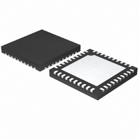
MAX15035ETL+ Maxim Integrated Products, MAX15035ETL+ Datasheet - Page 25

MAX15035ETL+
Manufacturer Part Number
MAX15035ETL+
Description
IC REG STEP DOWN 15A 40-TQFN
Manufacturer
Maxim Integrated Products
Type
Step-Down (Buck)r
Datasheet
1.MAX15035ETL.pdf
(26 pages)
Specifications of MAX15035ETL+
Internal Switch(s)
Yes
Synchronous Rectifier
Yes
Number Of Outputs
1
Voltage - Output
1.05V, 1.5V
Current - Output
15A
Voltage - Input
4.5 ~ 26 V
Operating Temperature
-40°C ~ 85°C
Mounting Type
Surface Mount
Package / Case
40-TQFN Exposed Pad
Power - Output
2.16W
Lead Free Status / RoHS Status
Lead free / RoHS Compliant
Frequency - Switching
-
Lead Free Status / Rohs Status
Lead free / RoHS Compliant
Calculating again with h = 1 gives the absolute limit of
dropout:
Therefore, V
very large output capacitance, and a practical input volt-
age with reasonable output capacitance would be 2.0V.
Careful PCB layout is critical to achieve low switching
losses and clean, stable operation. The switching
power stage requires particular attention. If possible,
mount all the power components on the top side of the
board with their ground terminals flush against one
another. Follow these guidelines for good PCB layout:
1) Keep the high-current paths short, especially at the
2) Connect all analog grounds to a separate solid
3) Keep the power traces and load connections short.
15A Step-Down Regulator with Internal Switches
ground terminals. This is essential for stable, jitter-
free operation.
copper plane, which connects to the GND pin of
the Quick-PWM controller. This includes the V
bypass capacitor, REF bypass capacitors, REFIN
components, and feedback compensation/dividers.
This is essential for high efficiency. The use of thick
V
V
IN MIN
IN MIN
(
(
)
)
IN
=
=
must be greater than 1.84V, even with
⎡
⎢
⎣ ⎣
⎡
⎢
⎣ ⎣
Applications Information
1 1 5 350
1 1 0 350
−
−
______________________________________________________________________________________
( .
( .
3 3
3 3
.
.
V
V
×
×
−
−
PCB Layout Guidelines
0
0
V
V
ns
ns
+
+
150
150
×
×
300
300
mV
mV
kHz
kHz
)
)
⎤
⎥ = 3 74
⎦
⎤
⎥ = 3 52
⎦
.
.
V
V
CC
4) Keep the power plane—especially LX—away from
1) Place the power components first, with ground ter-
2) Make the DC-DC controller ground connections as
3) Connect the output power planes (V
copper PCB (2oz vs. 1oz) can enhance full-load
efficiency by 1% or more. Correctly routing PCB
traces is a difficult task that must be approached in
terms of fractions of centimeters, where a single
milliohms of excess trace resistance causes a mea-
surable efficiency penalty.
sensitive analog areas (REF, REFIN, FB, ILIM).
minals adjacent (C
all these connections on the top layer with wide,
copper-filled areas.
shown in Figure 1. This diagram can be viewed as
having four separate ground planes: input/output
ground, where all the high-power components go;
the power ground plane, where the PGND pin and
V
ground plane where sensitive analog components,
the controller’s GND pin, and V
go. The controller’s GND plane must meet the
PGND plane only at a single point directly beneath
the IC. This point must also be very close to the out-
put capacitor ground terminal.
tem ground planes) directly to the output filter
capacitor positive and negative terminals with multi-
ple vias. Place the entire DC-DC converter circuit
as close to the load as is practical.
DD
bypass capacitor go; the controller’s analog
IN
and C
OUT
Layout Procedure
CC
). If possible, make
bypass capacitor
CORE
and sys-
25


