LTC3429BES6#TRPBF Linear Technology, LTC3429BES6#TRPBF Datasheet
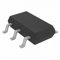
IC CONV DC/DC SYNC STPUPTSOT23-6

LTC3429BES6#TRPBF

Manufacturer Part Number
LTC3429BES6#TRPBF
Description
IC CONV DC/DC SYNC STPUPTSOT23-6
Manufacturer
Linear Technology
Type
Step-Up (Boost)r
Datasheet

Specifications of LTC3429BES6#TRPBF

Internal Switch(s)
Yes
Synchronous Rectifier
Yes
Number Of Outputs
1
Voltage - Output
2.5 ~ 4.3 V
Current - Output
600mA
Frequency - Switching
500kHz
Voltage - Input
0.5 ~ 4.4 V
Operating Temperature
-40°C ~ 85°C
Mounting Type
Surface Mount
Package / Case
TSOT-23-6, TSOT-6
Lead Free Status / RoHS Status
Lead free / RoHS Compliant
Power - Output
-

Available stocks

Company
Part Number
Manufacturer
Quantity
Price
Company:
Part Number:
LTC3429BES6#TRPBFLTC3429BES6
Manufacturer:
LT
Quantity:
10 000
Company:
Part Number:
LTC3429BES6#TRPBFLTC3429BES6
Manufacturer:
LT/凌特
Quantity:
20 000
Company:
Part Number:
LTC3429BES6#TRPBFLTC3429BES6#TR
Manufacturer:
LT
Quantity:
520
Company:
Part Number:
LTC3429BES6#TRPBF
Manufacturer:
LINEAR/凌特
Quantity:
20 000
FEATURES
TYPICAL APPLICATIO
APPLICATIO S
Up to 96% Efficiency
True Output Load Disconnect
Inrush Current Limiting and Internal Soft-Start
Low Voltage Start-Up: 0.85V
Automatic Burst Mode
Continuous Switching at Light Loads (LTC3429B)
Internal Synchronous Rectifier
Current Mode Control with Internal Compensation
Short-Circuit Protection
500kHz Fixed Frequency Switching
Input Range: 0.5V to 4.4V
Output Range: 2.5V to 4.3V (Up to 5V with Schottky)
Shutdown Current: <1µA
Antiringing Control Minimizes EMI
Tiny External Components
Low Profile (1mm) SOT-23 Package
MP3 Players
Digital Cameras
LCD Bias Supplies
Handheld Instruments
Wireless Handsets
GPS Receivers
+
Figure 1. 2-Cell to 3.3V Synchronous Boost Converter
2-CELL
AA
U
4.7µF
OFF ON
®
Operation with I
4.7µH
V
SHDN
IN
LTC3429
GND
SW
U
V
OUT
FB
1.02M
604k
Q
~ 20µA
3429 F01a
10µF
V
3.3V
250mA
OUT
Synchronous Boost Converter
600mA, 500kHz Micropower
DESCRIPTIO
The LTC
nous, fixed frequency, step-up DC/DC converters with true
output load disconnect, inrush current limiting and soft-
start in a low profile 6-lead ThinSOT
devices are capable of supplying 100mA from a single AA
cell input or 250mA from a 2-cell AA with a 3.3V output.
A switching frequency of 500kHz minimizes overall solu-
tion footprint by allowing the use of tiny, low profile
inductors and ceramic capacitors. Current mode PWM
control with internal compensation reduces external parts
count thereby saving critical board real estate. The LTC3429
shifts automatically to power saving Burst Mode operation
at light loads while the LTC3429B features continuous
switching at light loads. Antiringing control circuitry re-
duces EMI concerns by damping the inductor in discon-
tinuous mode.
The devices also feature low shutdown current of under
1µA. The true output disconnect feature allows the output
to be completely discharged in shutdown. It also limits the
inrush of current during start-up, minimizing surge cur-
rents seen by the input supply.
trademarks are the property of their respective owners. Burst Mode is a registered
trademark of Linear Technology Corporation. ThinSOT is a trademark of Linear Technology
Corporation.
, LTC and LT are registered trademarks of Linear Technology Corporation. All other
with Output Disconnect
®
3429/LTC3429B are high efficiency synchro-
100
90
80
70
60
50
40
0.1
LTC3429/LTC3429B
EFFICIENCY
U
2-Cell to 3.3V Efficiency
1
OUTPUT CURRENT (mA)
10
V
POWER LOSS
V
IN
IN
V
= 2.4V
IN
= 2.4V
TM
= 3V
100
package. These
V
IN
= 3V
3429 F01b
1000
100
10
1
0.1
0.01
0.001
0.0001
3429fa
1

Related parts for LTC3429BES6#TRPBF

LTC3429BES6#TRPBF Summary of contents

Page 1

... LTC and LT are registered trademarks of Linear Technology Corporation. All other trademarks are the property of their respective owners. Burst Mode is a registered trademark of Linear Technology Corporation. ThinSOT is a trademark of Linear Technology Corporation ...

Page 2

LTC3429/LTC3429B ABSOLUTE AXI U RATI GS (Note 1) V Voltage .............................................. – 0. Voltage ................................................. – 0. SHDN, FB Voltage ....................................... – 0. ........................................................... – 0. ...

Page 3

W U TYPICAL PERFOR A CE CHARACTERISTICS Single-Cell to 3.3V Efficiency (LTC3429 Only) 100 1.5V IN EFFICIENCY POWER LOSS 40 0.1 ...

Page 4

LTC3429/LTC3429B W U TYPICAL PERFOR A CE CHARACTERISTICS Output Voltage vs Temperature 3. 1. 30mA OUT 3.40 3.36 3.32 3.28 3.24 3.20 3.16 –60 –40 – 100 TEMPERATURE (°C) 3429 ...

Page 5

CTIO S SW (Pin 1): Switch Pin. Connect inductor between SW and V . Keep these PCB trace lengths as short and wide IN as possible to reduce EMI and voltage overshoot. If the inductor ...

Page 6

LTC3429/LTC3429B U OPERATIO The LTC3429/LTC3429B are 500kHz, synchronous boost converters housed in a 6-lead SOT-23 package. Able to operate from an input voltage below 1V, the device fea- tures fixed frequency, current mode PWM control for exceptional line and load ...

Page 7

U OPERATIO Thermal Shutdown An internal temperature monitor will start to reduce the peak current limit if the die temperature exceeds 125°C. If the die temperature continues to rise and reaches 160°C, the part will go into thermal shutdown, all ...

Page 8

LTC3429/LTC3429B U OPERATIO is achieved by terminating the switching of the synchro- nous PMOS and applying V statically on its gate. This IN ensures that the slope of the inductor current will reverse during the time current is flowing to ...

Page 9

U U APPLICATIO S I FOR ATIO The inductor current ripple is typically set for 20% to 40% of the maximum inductor current (I ferrite core inductor materials reduce frequency dependent power losses compared to cheaper powdered iron types, improving ...

Page 10

LTC3429/LTC3429B U TYPICAL APPLICATIO S Applications Where V > 4.3V OUT When the output voltage is programmed above 4.3V necessary to add a Schottky diode either from add a snubber network in order ...

Page 11

... MOLD FLASH SHALL NOT EXCEED 0.254mm 6. JEDEC PACKAGE REFERENCE IS MO-193 Information furnished by Linear Technology Corporation is believed to be accurate and reliable. However, no responsibility is assumed for its use. Linear Technology Corporation makes no represen- tation that the interconnection of its circuits as described herein will not infringe on existing patent rights. U ...

Page 12

... Synchronous Step-Up DC/DC SW Converter with Output Disconnect LT3464 85mA (I ), High Efficiency Step-Up DC/DC Converter SW with Integrated Schottky and PNP Disconnect trademark of Linear Technology Corporation. SENSE Linear Technology Corporation 12 1630 McCarthy Blvd., Milpitas, CA 95035-7417 (408) 432-1900 FAX: (408) 434-0507 ● + ...

Related keywords