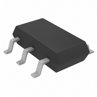
LTC3429BES6#TRPBF Linear Technology, LTC3429BES6#TRPBF Datasheet - Page 2

LTC3429BES6#TRPBF
Manufacturer Part Number
LTC3429BES6#TRPBF
Description
IC CONV DC/DC SYNC STPUPTSOT23-6
Manufacturer
Linear Technology
Type
Step-Up (Boost)r
Datasheet
1.LTC3429ES6TRMPBF.pdf
(12 pages)
Specifications of LTC3429BES6#TRPBF
Internal Switch(s)
Yes
Synchronous Rectifier
Yes
Number Of Outputs
1
Voltage - Output
2.5 ~ 4.3 V
Current - Output
600mA
Frequency - Switching
500kHz
Voltage - Input
0.5 ~ 4.4 V
Operating Temperature
-40°C ~ 85°C
Mounting Type
Surface Mount
Package / Case
TSOT-23-6, TSOT-6
Lead Free Status / RoHS Status
Lead free / RoHS Compliant
Power - Output
-
Available stocks
Company
Part Number
Manufacturer
Quantity
Price
ABSOLUTE AXI U RATI GS
LTC3429/LTC3429B
(Note 1)
V
SW Voltage ................................................. – 0.3V to 6V
SHDN, FB Voltage ....................................... – 0.3V to 6V
V
Operating Temperature Range (Note 2) .. – 40°C to 85°C
Storage Temperature Range ................... – 65°C to 150°
Lead Temperature (Soldering, 10 sec).................. 300°C
ELECTRICAL CHARACTERISTICS
Note 1: Absolute Maximum Ratings are those values beyond which the life
of a device may be impaired.
Note 2: The LTC3429ES6/LTC3429BES6 are guaranteed to meet
performance specifications from 0°C to 70°C. Specifications over the
–40°C to 85°C operating temperature range are assured by design,
characterization and correlation with statistical process controls.
2
temperature range, otherwise specifications are at T
PARAMETER
Minimum Start-Up Voltage
Minimum Operating Voltage
Output Voltage Adjust Range
Feedback Voltage
Feedback Input Current
Quiescent Current (Burst Mode Operation)
Quiescent Current (Shutdown)
Quiescent Current (Active)
NMOS Switch Leakage
PMOS Switch Leakage
NMOS Switch On Resistance
PMOS Switch On Resistance
NMOS Current Limit
Burst Mode Operation Current Threshold
Current Limit Delay to Output
Max Duty Cycle
Switching Frequency
SHDN Input High
SHDN Input Low
SHDN Input Current
Soft-Start Time
IN
OUT
Voltage .............................................. – 0.3V to 4.4V
........................................................... – 0.3V to 6V
W
W W
CONDITIONS
I
SHDN = V
(Note 5)
V
V
V
Measured on V
V
V
L = 4.7µH (LTC3429 Only)
V
V
LOAD
FB
FB
SHDN
SW
SW
FB
SHDN
SHDN to 90% of V
= 1.25V
= 1.4V (Note 4)
= 1.15V
= 5V
= 5V, V
U
= 1mA, V
= 0V, Not Including Switch Leakage, V
= 5.5V
A
= 25°C. V
IN
OUT
(Note 3)
The
OUT
OUT
= 0V
, Nonswitching
= 0V
●
IN
OUT
denotes the specifications which apply over the full operating
= 1.2V, V
PACKAGE/ORDER I FOR ATIO
Consult LTC Marketing for parts specified with wider operating temperature ranges.
Note 3: Minimum V
battery’s ability to provide the necessary power as it enters a deeply
discharged state.
Note 4: Burst Mode operation I
by V
Note 5: For applications where V
required. See the Applications Information.
OUT
GND 2
OUT
SW 1
FB 3
T
/V
6-LEAD PLASTIC TSOT-23
JMAX
IN
= 3.3V, unless otherwise specified.
to get the equivalent input (battery) current.
= 125°C, θ
S6 PACKAGE
TOP VIEW
OUT
IN
JC
operation after start-up is only limited by the
= 0V
= 102°C/W
6 V
5 V
4 SHDN
IN
OUT
Q
●
●
●
OUT
is measured at V
1.192
> 4.3V, an external Schottky diode is
MIN
600
380
2.5
80
1
U
S6 PART MARKING
1.230
LTC3429ES6
LTC3429BES6
0.85
0.01
0.35
0.45
1.25
0.01
ORDER PART
TYP
380
850
500
0.5
0.1
0.1
2.5
20
40
90
1
OUT
NUMBER
. Multiply this value
LTH5
LTBMS
W
1.268
MAX
0.65
0.35
550
620
50
30
1
5
1
5
5
1
UNITS
U
3429fa
kHz
mA
mA
ms
nA
µA
µA
µA
µA
µA
µA
ns
%
Ω
Ω
V
V
V
V
V
V


