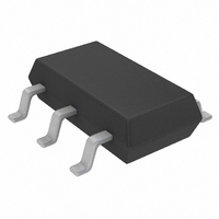
LTC3429BES6#TRPBF Linear Technology, LTC3429BES6#TRPBF Datasheet - Page 8

LTC3429BES6#TRPBF
Manufacturer Part Number
LTC3429BES6#TRPBF
Description
IC CONV DC/DC SYNC STPUPTSOT23-6
Manufacturer
Linear Technology
Type
Step-Up (Boost)r
Datasheet
1.LTC3429ES6TRMPBF.pdf
(12 pages)
Specifications of LTC3429BES6#TRPBF
Internal Switch(s)
Yes
Synchronous Rectifier
Yes
Number Of Outputs
1
Voltage - Output
2.5 ~ 4.3 V
Current - Output
600mA
Frequency - Switching
500kHz
Voltage - Input
0.5 ~ 4.4 V
Operating Temperature
-40°C ~ 85°C
Mounting Type
Surface Mount
Package / Case
TSOT-23-6, TSOT-6
Lead Free Status / RoHS Status
Lead free / RoHS Compliant
Power - Output
-
Available stocks
Company
Part Number
Manufacturer
Quantity
Price
OPERATIO
APPLICATIO S I FOR ATIO
LTC3429/LTC3429B
PCB LAYOUT GUIDELINES
The high speed operation of the LTC3429/LTC3429B
demands careful attention to board layout. You will not get
advertised performance with careless layout. Figure 2
shows the recommended component placement. A large
ground pin copper area will help to lower the chip tempera-
ture. A multilayer board with a separate ground plane is
ideal, but not absolutely necessary.
COMPONENT SELECTION
Inductor Selection
The LTC3429/LTC3429B can utilize small surface mount
and chip inductors due to its fast 500kHz switching
frequency. Typically, a 4.7µH inductor is recommended
for most applications. Larger values of inductance will
allow greater output current capability by reducing the
8
is achieved by terminating the switching of the synchro-
nous PMOS and applying V
ensures that the slope of the inductor current will reverse
during the time current is flowing to the output. Since the
PMOS no longer acts as a low impedance switch in this
Figure 2. Recommended Component Placement
for Single Layer Board
RECOMMENDED COMPONENT PLACEMENT. TRACES
CARRYING HIGH CURRENT ARE DIRECT. TRACE AREA AT
FB PIN IS SMALL. LEAD LENGTH TO BATTERY IS SHORT
V
IN
U
U
U
1
2
3
IN
SW
GND
FB
statically on its gate. This
SHDN
3429 F02
V
OUT
V
W
IN
V
OUT
6
5
4
SHDN
U
mode, there will be more power dissipation within the IC.
This will cause a sharp drop in the efficiency (see Typical
Performance Characteristics, Efficiency vs V
mum output current should be limited in order to maintain
an acceptable junction temperature.
inductor ripple current. Increasing the inductance above
10µH will increase size while providing little improvement
in output current capability.
The approximate output current capability of the LTC3429
versus inductance value is given in the equation below and
illustrated graphically in Figure 3.
where:
η = estimated efficiency
I
V
D = steady-state duty ratio = (V
f = switching frequency (500kHz typical)
L = inductance value
I
P
OUT MAX
IN
= peak current limit value (0.6A)
= input (battery) voltage
(
200
180
160
140
120
100
80
60
40
20
)
0
Figure 3. Maximum Output Current vs
Inductance Based on 90% Efficiency
3
=
V
IN
η
5
= 1.2V
•
⎛
⎜
⎝
7
I
P
9
–
INDUCTANCE (µH)
f L
11
V
• •
IN
13
•
V
V
D
OUT
OUT
2
15 17
⎞
⎟
⎠
= 3.3V
= 5V
• –
OUT
(
1
19
– V
D
21
3429 F03
)
IN
23
IN
)/V
). The maxi-
OUT
3429fa


