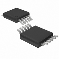
LTC1700EMS Linear Technology, LTC1700EMS Datasheet

LTC1700EMS
Specifications of LTC1700EMS
Available stocks
Related parts for LTC1700EMS
LTC1700EMS Summary of contents
Page 1
... Cellular Telephones ■ Wireless Modems ■ RF Communications ■ 2.5V to 3.3V, 2. Converters ■ Battery-Powered Equipment ■ Telecom/Network Systems , LTC and LT are registered trademarks of Linear Technology Corporation. Burst Mode, OPTI-LOOP are registered trademarks of Linear Technology Corporation trademark of Linear Technology Corporation. SENSE U TYPICAL APPLICATIO ...
Page 2
... OUT V = 1.8V 1.8V 1.1V OUT RUN/ Ramping Down from 1.2V SYNC/MODE f = 550kHz OSC V = 1.8V OUT ± 10mV FB REF ORDER PART NUMBER 10 SW LTC1700EMS 9 PGND OUT PART MARKING = 150°C/W JA LTLC MIN TYP MAX UNITS 0.9 1.8 2.34 2 536 620 179 210 ...
Page 3
ELECTRICAL CHARACTERISTICS temperature range, otherwise specifications are at T SYMBOL PARAMETER TG Transition Time Gate Drive Rise Time Gate Drive Fall Time f BG Transition Time Gate Drive Rise Time ...
Page 4
LTC1700 W U TYPICAL PERFORMANCE CHARACTERISTICS RUN/SS Current vs Temperature 105 – 55 –35 – 125 TEMPERATURE (°C) 1700 G04 Maximum Current Sense Voltage vs Temperature 90 80 ...
Page 5
W U TYPICAL PERFORMANCE CHARACTERISTICS Load Step Transient Response Burst Mode Operation Inhibited A/C COUPLED OUTPUT VOLTAGE (0.2V/DIV) INDUCTOR CURRENT (2A/DIV) 2A/DIV SYNC LOAD STEP = 100mA TO 1.7A OUT ...
Page 6
LTC1700 U U FUNCTIONAL DIAGRA “0” ONLY WHEN CONSTANT “1”, OTHERWISE Y = “1” BURST INHIBIT X SYNC/ 5 MODE MAIN OSC – 1.205V + Ω g ...
Page 7
U OPERATIO output feedback voltage V . When the load current in- FB creases, it causes a slight decreases in V 1.205V reference, which in turn causes the I increase until the average inductor current matches the new load current. ...
Page 8
LTC1700 U U APPLICATIONS INFORMATION Power MOSFET Selection The LTC1700 requires two external power MOSFETs, one for the main switch (N-channel) and one for the synchro- nous rectifier (P-channel). Since the voltage operating range of the LTC1700 is limited to ...
Page 9
U U APPLICATIONS INFORMATION load current. When the LTC1700 is operating in continu- ous mode, the duty cycles for the MOSFETs are: Main MOSFET Duty Cycle = 1 – V Synchronous MOSFET Duty Cycle = V The MOSFET power dissipations ...
Page 10
LTC1700 U U APPLICATIONS INFORMATION To eliminate this subharmonic oscillation, a compensat- ing ramp is added internally to the LTC1700 on the inductor current waveform when the duty cycle exceeds 5%. This scheme, known as slope compensation, makes the loop ...
Page 11
U U APPLICATIONS INFORMATION preferred at high switching frequencies, so design goals can concentrate on copper loss and preventing saturation. Ferrite core material saturates “hard”, which means that inductance collapses abruptly when the peak design cur- rent is exceeded. This ...
Page 12
LTC1700 U U APPLICATIONS INFORMATION The efficiency of a switching regulator is equal to the output power divided by the input power (× 100%). Percent efficiency can be expressed as: % Efficiency = 100%–( ...) ...
Page 13
U U APPLICATIONS INFORMATION where Voltage drop of P-channel parasitic diode Initial load current during start-up OUT C = Output capacitance OUT Hence you would select the start-up capacitor, C ensure t > t Remember ...
Page 14
LTC1700 U U APPLICATIONS INFORMATION 3.9nF 5k 270pF 470pF 100k 316k C1, C3: TAIYO YUDEN CERAMIC JMK316BJ106ML C2: AVX TAJB68K006R C4: SANYO POSCAP 6TPB470M PC Board Layout Checklist When laying out the printed circuit board, the following checklist should be ...
Page 15
... TYP RECOMMENDED SOLDER PAD LAYOUT Information furnished by Linear Technology Corporation is believed to be accurate and reliable. However, no responsibility is assumed for its use. Linear Technology Corporation makes no represen- tation that the interconnection of its circuits as described herein will not infringe on existing patent rights. L1 1.5µH ...
Page 16
... V OUT + 3.3V/1. 220µF 22µF 6.3V 1700 • TA02 ; Precise Control of Peak Switch Current IN Q ≤ 36V; IN ≤ 15A OUT IN OUT ≤ 30V Programmable Frequency IN SENSE LT/TP 0804 1K REV A • PRINTED IN USA © LINEAR TECHNOLOGY CORPORATION 2000 1700fa ...


