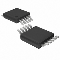
LTC1700EMS Linear Technology, LTC1700EMS Datasheet - Page 8

LTC1700EMS
Manufacturer Part Number
LTC1700EMS
Description
IC DC/DC CONTRLR STP-UP 10-MSOP
Manufacturer
Linear Technology
Type
Step-Up (Boost)r
Datasheet
1.LTC1700EMS.pdf
(16 pages)
Specifications of LTC1700EMS
Internal Switch(s)
No
Synchronous Rectifier
Yes
Number Of Outputs
1
Current - Output
1A
Frequency - Switching
530kHz
Voltage - Input
0.9 ~ 6 V
Operating Temperature
-40°C ~ 85°C
Mounting Type
Surface Mount
Package / Case
10-MSOP, Micro10™, 10-uMAX, 10-uSOP
Lead Free Status / RoHS Status
Contains lead / RoHS non-compliant
Voltage - Output
-
Power - Output
-
Available stocks
Company
Part Number
Manufacturer
Quantity
Price
Company:
Part Number:
LTC1700EMS
Manufacturer:
LT
Quantity:
10 000
Part Number:
LTC1700EMS
Manufacturer:
LINEAR/凌特
Quantity:
20 000
Part Number:
LTC1700EMS#PBF
Manufacturer:
LT凌特厂
Quantity:
20 000
LTC1700
Power MOSFET Selection
The LTC1700 requires two external power MOSFETs, one
for the main switch (N-channel) and one for the synchro-
nous rectifier (P-channel). Since the voltage operating
range of the LTC1700 is limited to less than 6V, the
breakdown voltage of the MOSFETs is not a concern.
Therefore the MOSFETs parameters that should be used
for selecting the power MOSFETs are threshold voltage
V
tance C
The gate drive voltage is set by the output voltage, V
Since the LTC1700 exits the start-up mode at 2.3V, sub-
logic level threshold MOSFETs should be used in LTC1700
applications. Newer MOSFETs with guaranteed R
gate voltage of 1.8V are now available and will work very
well with the LTC1700.
The MOSFETs on-resistance is chosen based on the
required load current. The maximum average output
current I
where:
The peak inductor current is inherently limited in a
current mode controller. The maximum V
age of the main MOSFET is limited to 78mV. The LTC1700
will not allow peak inductor current to exceed 78mV/
R
guide for determining the required R
ing some margin for ripple current, current limit and
variations in the LTC1700 and external component val-
ues:
8
APPLICATIONS
GS(TH)
DS(ON)(N-CHANNEL)
I
I
∆I = Inductor Ripple Current
DC = Duty Cycle
R
O(MAX)
PK
DS ON MAX
= Peak Inductor Current
(
, on-resistance R
RSS
O(MAX)
)(
= (I
and maximum current I
PK
)
is :
– 0.5∆I)(1 – DC)
≅
. The following equation is a good
⎛
⎜
⎝
U
I
1
O MAX
(
–
DC
DS(ON)
INFORMATION
U
∆
)
V
+
SENSE
, reverse transfer capaci-
2
1
∆
I
L
W
D(MAX)
⎞
⎟
⎠
DS(ON)(MAX)
( )
ρ
T
DS
.
sense volt-
U
, allow-
DSON
OUT
at
.
For 25°C operating condition, set ∆V
conditions that vary over the full temperature range, set
∆V
The ρ
variation in R
0.375%/°C as shown in Figure 2. Junction to case tem-
perature T
maximum ambient temperature of 70°C, using ρ
in the above equation is a reasonable choice. This equation
is plotted in Figure 3 to illustrate the dependence of
maximum output current on R
∆I = 0.4I
Power dissipated by the main and synchronous
MOSFETs depends upon their respective duty cycles and
SENSE
T
is a normalized term accounting for the significant
O(MAX)
= 55mV.
JC
1.5
1.4
1.3
1.2
1.1
1.0
0.9
0.8
0.7
0.6
5.0
4.5
4.0
3.5
3.0
2.5
2.0
1.5
1.0
0.5
is around 10°C in most applications. For a
0
–55
Figure 3. Maximum Current vs R
DS(ON)
0
.
Figure 2. R
–35
10 20 30 40 50 60 70 80 90 100
DUTY CYCLE = 10%
–15
with temperature, typically about
TEMPERATURE (°C)
5
DUTY CYCLE = 50%
DS(ON)
R
DS(ON)
25
DUTY CYCLE = 80%
45
(mΩ)
vs Temperature
65
DS(ON)
85 105
SENSE
1700 F02
1700 F03
DS(ON)
125
, assuming
= 65mV. For
80°C
≅ 1.2
1700fa


