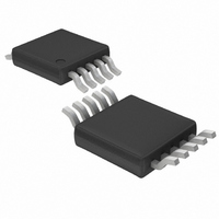
LTC1700EMS Linear Technology, LTC1700EMS Datasheet - Page 5

LTC1700EMS
Manufacturer Part Number
LTC1700EMS
Description
IC DC/DC CONTRLR STP-UP 10-MSOP
Manufacturer
Linear Technology
Type
Step-Up (Boost)r
Datasheet
1.LTC1700EMS.pdf
(16 pages)
Specifications of LTC1700EMS
Internal Switch(s)
No
Synchronous Rectifier
Yes
Number Of Outputs
1
Current - Output
1A
Frequency - Switching
530kHz
Voltage - Input
0.9 ~ 6 V
Operating Temperature
-40°C ~ 85°C
Mounting Type
Surface Mount
Package / Case
10-MSOP, Micro10™, 10-uMAX, 10-uSOP
Lead Free Status / RoHS Status
Contains lead / RoHS non-compliant
Voltage - Output
-
Power - Output
-
Available stocks
Company
Part Number
Manufacturer
Quantity
Price
Company:
Part Number:
LTC1700EMS
Manufacturer:
LT
Quantity:
10 000
Part Number:
LTC1700EMS
Manufacturer:
LINEAR/凌特
Quantity:
20 000
Part Number:
LTC1700EMS#PBF
Manufacturer:
LT凌特厂
Quantity:
20 000
PIN
SGND (Pin 1): Small-Signal Ground. Must be routed
separately from other grounds to the (–) terminal of C
I
current comparator threshold increases with this control
voltage. Nominal voltage range for this pin is 0V to 1.18V.
V
nal resistive divider across the output capacitor.
RUN/SS (Pin 4): Combination of Soft-Start and Run
Control Inputs. A capacitor to ground at this pin sets the
ramp time to full output current. The time is approximately
0.45s/µF. Forcing this pin below 1.08V causes all circuitry
to be shut down.
SYNC/MODE (Pin 5): This pin performs three functions. A
voltage greater than 1.2V on this pin allows Burst Mode
operation at low load currents, while grounding or apply-
ing a clock signal on this pin defeats Burst Mode operation.
An external clock between 400kHz and 750kHz applied to
this pin forces the LTC1700 to operate at the external clock
frequency. Do not attempt to synchronize below 400kHz
or above 750kHz.
TYPICAL PERFORMANCE CHARACTERISTICS
A/C COUPLED
TH
INDUCTOR
FB
CURRENT
(0.2V/DIV)
VOLTAGE
(2A/DIV)
U
OUTPUT
(Pin 2): Error Amplifier Compensation Point. The
(Pin 3): Receives the feedback voltage from an exter-
FUNCTIONS
Load Step Transient Response
Burst Mode Operation Inhibited
V
V
IN
OUT
U
= 3.3V
= 5V
V
LOAD STEP = 100mA TO 1.7A
SYNC
U
= 0V
2A/DIV
W
U
1700 G13
A/C COUPLED
INDUCTOR
(0.2V/DIV)
CURRENT
VOLTAGE
(2A/DIV)
OUTPUT
Load Step Transient Response
Burst Mode Operation Enabled
V
V
IN
OUT
= 4.2V
= 5V
OUT
.
V
LOAD STEP = 100mA TO 1.7A
SYNC
TG (Pin 6): Top Gate Drive. Drives the external synchro-
nous P-channel MOSFET with a voltage swing between 0V
to V
V
the supply pin and also as one of the inputs to the current
reversal comparator.
BG (Pin 8): Bottom Gate Drive. Drives the external main
N-channel MOSFET with a voltage swing between 0V to
V
PGND (Pin 9): Top and Bottom Gate Drivers Ground.
Connects to the (–) terminal of C
N-channel MOSFET must be connected close to this pin
since this pin is also one of the inputs to the V
amplifier.
SW (Pin 10): This pin connects to the inputs of two
comparators: The V
reversal comparator. The drain of an internal N-channel
start-up MOSFET (M1) is also connected to this pin.
= V
2A/DIV
OUT
OUT
IN
OUT
.
(Pin 7): This pin performs two functions. It serves as
.
1700 G14
A/C COUPLED
INDUCTOR
CURRENT
(0.2V/DIV)
DS
VOLTAGE
(2A/DIV)
OUTPUT
sense amplifier and the current
Load Step Transient Response
Burst Mode Operation Inhibited
V
V
IN
OUT
= 4.2V
= 5V
OUT
V
LOAD STEP = 100mA TO 1.7A
SYNC
. Source of the main
= 0V
LTC1700
2A/DIV
DS
sense
1700fa
5
1700 G15


