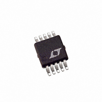
LTC3407EMSE Linear Technology, LTC3407EMSE Datasheet - Page 5

LTC3407EMSE
Manufacturer Part Number
LTC3407EMSE
Description
IC REG DC/DC DUAL 1.5MHZ 10-MSOP
Manufacturer
Linear Technology
Type
Step-Down (Buck)r
Datasheet
1.LTC3407EMSE.pdf
(16 pages)
Specifications of LTC3407EMSE
Internal Switch(s)
Yes
Synchronous Rectifier
Yes
Number Of Outputs
2
Voltage - Output
0.6 ~ 5 V
Current - Output
1A
Frequency - Switching
1.5MHz
Voltage - Input
2.5 ~ 5.5 V
Operating Temperature
-40°C ~ 85°C
Mounting Type
Surface Mount
Package / Case
10-MSOP Exposed Pad, 10-HMSOP, 10-eMSOP
Lead Free Status / RoHS Status
Contains lead / RoHS non-compliant
Power - Output
-
Available stocks
Company
Part Number
Manufacturer
Quantity
Price
Company:
Part Number:
LTC3407EMSE
Manufacturer:
LT
Quantity:
10 000
Part Number:
LTC3407EMSE
Manufacturer:
LT
Quantity:
20 000
Company:
Part Number:
LTC3407EMSE#TR
Manufacturer:
LTC
Quantity:
2 576
Part Number:
LTC3407EMSE#TR
Manufacturer:
LINEAR/凌特
Quantity:
20 000
Company:
Part Number:
LTC3407EMSE#TRPBF
Manufacturer:
LTC
Quantity:
1 388
Part Number:
LTC3407EMSE#TRPBF
Manufacturer:
LT/凌特
Quantity:
20 000
Company:
Part Number:
LTC3407EMSE-1
Manufacturer:
LT
Quantity:
10 000
Company:
Part Number:
LTC3407EMSE-2
Manufacturer:
LT
Quantity:
10 000
Part Number:
LTC3407EMSE-2
Manufacturer:
LTNEAR
Quantity:
20 000
Part Number:
LTC3407EMSE-2#TR
Manufacturer:
LT/凌特
Quantity:
20 000
PIN FUNCTIONS
TYPICAL PERFORMANCE CHARACTERISTICS
V
age from the external resistive divider across the output.
Nominal voltage for this pin is 0.6V.
RUN1 (Pin 2): Regulator 1 Enable. Forcing this pin to V
enables regulator 1, while forcing it to GND causes regulator
1 to shut down. This pin must be driven; do not fl oat.
V
to GND.
SW1 (Pin 4): Regulator 1 Switch Node Connection to the
Inductor. This pin swings from V
GND (Pin 5): Ground. This pin is not connected internally.
Connect to PCB ground for shielding.
MODE/SYNC (Pin 6): Combination Mode Selection and
Oscillator Synchronization. This pin controls the opera-
tion of the device. When tied to V
operation or pulse-skipping mode is selected, respectively.
Do not fl oat this pin. The oscillation frequency can be
FB1
IN
100
95
90
85
80
75
70
65
60
(Pin 3): Main Power Supply. Must be closely decoupled
(Pin 1): Output Feedback. Receives the feedback volt-
Effi ciency vs Load Current
1
V
CIRCUIT OF FIGURE 1
OUT
LOAD CURRENT (mA)
10
= 1.2V Burst Mode OPERATION
4.2V
3.3V
100
2.7V
3407 G13
IN
IN
1000
to GND.
or GND, Burst Mode
100
95
90
85
80
75
70
65
60
Effi ciency vs Load Current
1
V
CIRCUIT OF FIGURE 1
OUT
LOAD CURRENT (mA)
10
IN
= 1.5V Burst Mode OPERATION
3.3V
4.2V
synchronized to an external oscillator applied to this pin
and pulse-skipping mode is automatically selected.
SW2 (Pin 7): Regulator 2 Switch Node Connection to the
Inductor. This pin swings from V
POR (Pin 8): Power-On Reset . This common-drain logic
output is pulled to GND when the output voltage is not
within ±8.5% of regulation and goes high after 175ms
when both channels are within regulation.
RUN2 (Pin 9): Regulator 2 Enable. Forcing this pin to V
enables regulator 2, while forcing it to GND causes regulator
2 to shut down. This pin must be driven; do not fl oat.
V
voltage from the external resistive divider across the output.
Nominal voltage for this pin is 0.6V.
Exposed Pad (GND) (Pin 11): Power Ground. Connect to
the (–) terminal of C
soldered to electrical ground on PCB.
FB2
100
(Pin 10): Output Feedback. Receives the feedback
2.7V
3407 G14
1000
OUT
–0.1
–0.2
–0.3
–0.4
–0.5
0.5
0.4
0.3
0.2
0.1
0
, and (–) terminal of C
Line Regulation
2
V
I
T
OUT
OUT
A
= 25°C
= 200mA
= 1.8V
3
IN
to GND.
V
IN
LTC3407
4
(V)
IN
5
. Must be
3407 G15
3407fa
5
6
IN


