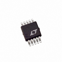
LTC3407EMSE Linear Technology, LTC3407EMSE Datasheet - Page 6

LTC3407EMSE
Manufacturer Part Number
LTC3407EMSE
Description
IC REG DC/DC DUAL 1.5MHZ 10-MSOP
Manufacturer
Linear Technology
Type
Step-Down (Buck)r
Datasheet
1.LTC3407EMSE.pdf
(16 pages)
Specifications of LTC3407EMSE
Internal Switch(s)
Yes
Synchronous Rectifier
Yes
Number Of Outputs
2
Voltage - Output
0.6 ~ 5 V
Current - Output
1A
Frequency - Switching
1.5MHz
Voltage - Input
2.5 ~ 5.5 V
Operating Temperature
-40°C ~ 85°C
Mounting Type
Surface Mount
Package / Case
10-MSOP Exposed Pad, 10-HMSOP, 10-eMSOP
Lead Free Status / RoHS Status
Contains lead / RoHS non-compliant
Power - Output
-
Available stocks
Company
Part Number
Manufacturer
Quantity
Price
Company:
Part Number:
LTC3407EMSE
Manufacturer:
LT
Quantity:
10 000
Part Number:
LTC3407EMSE
Manufacturer:
LT
Quantity:
20 000
Company:
Part Number:
LTC3407EMSE#TR
Manufacturer:
LTC
Quantity:
2 576
Part Number:
LTC3407EMSE#TR
Manufacturer:
LINEAR/凌特
Quantity:
20 000
Company:
Part Number:
LTC3407EMSE#TRPBF
Manufacturer:
LTC
Quantity:
1 388
Part Number:
LTC3407EMSE#TRPBF
Manufacturer:
LT/凌特
Quantity:
20 000
Company:
Part Number:
LTC3407EMSE-1
Manufacturer:
LT
Quantity:
10 000
Company:
Part Number:
LTC3407EMSE-2
Manufacturer:
LT
Quantity:
10 000
Part Number:
LTC3407EMSE-2
Manufacturer:
LTNEAR
Quantity:
20 000
Part Number:
LTC3407EMSE-2#TR
Manufacturer:
LT/凌特
Quantity:
20 000
The LTC3407 uses a constant frequency, current mode
architecture. The operating frequency is set at 1.5MHz
and can be synchronized to an external oscillator. Both
channels share the same clock and run in-phase. To suit
a variety of applications, the selectable Mode pin allows
the user to trade-off noise for effi ciency.
The output voltage is set by an external divider returned
to the V
output voltage with a reference voltage of 0.6V and adjusts
the peak inductor current accordingly. Overvoltage and
undervoltage comparators will pull the POR output low if
the output voltage is not within ±8.5%. The POR output
will go high after 262,144 clock cycles (about 175ms) of
achieving regulation.
LTC3407
BLOCK DIAGRAM
OPERATION
6
FB
pins. An error amplifi er compares the divided
MODE/SYNC
RUN1
RUN2
V
V
FB1
FB2
10
6
1
2
9
REGULATOR 1
0.6V REF
REGULATOR 2 (IDENTICAL TO REGULATOR 1)
0.55V
0.65V
0.6V
SHUTDOWN
+
–
–
+
+
–
UVDET
OVDET
OSC
EA
I
UV
OV
TH
OSC
0.35V
SLOPE
COMP
S
R
LATCH
–
+
RS
BURST
Q
Q
EN
SWITCHING
Main Control Loop
During normal operation, the top power switch (P-channel
MOSFET) is turned on at the beginning of a clock cycle
when the V
The current into the inductor and the load increases until
the current limit is reached. The switch turns off and
energy stored in the inductor fl ows through the bottom
switch (N-channel MOSFET) into the load until the next
clock cycle.
The peak inductor current is controlled by the internally
compensated I
ror amplifi er. This amplifi er compares the V
0.6V reference. When the load current increases, the
V
BLANKING
COUNTER
CIRCUIT
SLEEP
LOGIC
FB
POR
AND
PGOOD1
PGOOD2
voltage decreases slightly below the reference. This
–
I
FB
COMP
SHOOT-
I
THRU
ANTI
RCMP
voltage is below the the reference voltage.
+
TH
+
–
CLAMP
BURST
voltage, which is the output of the er-
5Ω
V
V
IN
IN
3407 BD
11
4
3
8
5
7
SW1
GND
V
POR
GND
SW2
IN
FB
pin to the
3407fa


