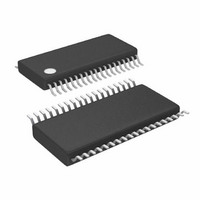
LTC3865EFE#TRPBF Linear Technology, LTC3865EFE#TRPBF Datasheet - Page 14

LTC3865EFE#TRPBF
Manufacturer Part Number
LTC3865EFE#TRPBF
Description
IC BUCK SYNC ADJ DUAL 38TSSOP
Manufacturer
Linear Technology
Type
Step-Down (Buck)r
Datasheet
1.LTC3865EUHPBF.pdf
(38 pages)
Specifications of LTC3865EFE#TRPBF
Internal Switch(s)
No
Synchronous Rectifier
Yes
Number Of Outputs
2
Voltage - Output
0.6 ~ 5 V
Frequency - Switching
250kHz ~ 770kHz
Voltage - Input
4.5 ~ 38 V
Operating Temperature
-40°C ~ 85°C
Mounting Type
Surface Mount
Package / Case
38-TSSOP Exposed Pad, 38-eTSSOP, 38-HTSSOP
Lead Free Status / RoHS Status
Lead free / RoHS Compliant
Current - Output
-
Power - Output
-
Available stocks
Company
Part Number
Manufacturer
Quantity
Price
LTC3865/LTC3865-1
OPERATION
bad mask is 100μs when there are any VID transitions.
On the LTC3865-1 (UH32 package) or the LTC3865 (FE38
package), each channel has its own PGOOD pin. Therefore,
the PGOOD pins now only respond to their own channels.
The PGOOD pins are allowed to be pulled up by external
resistors to sources of up to 6V.
Output Overvoltage Protection
An overvoltage comparator, OV, guards against transient
overshoots (>10%) as well as other more serious condi-
tions that may overvoltage the output. In such cases,
the top MOSFET is turned off and the bottom MOSFET is
turned on until the reverse current limit for the overvoltage
condition is reached. The bottom MOSFET will be turned on
again at the next clock and be turned off when the reverse
current limit is reached again. This process repeats until
the overvoltage condition is cleared.
APPLICATIONS INFORMATION
The Typical Application on the fi rst page is a basic LTC3865
application circuit. The LTC3865 can be confi gured to use
either DCR (inductor resistance) sensing or low value resis-
tor sensing. The choice between the two current sensing
schemes is largely a design trade-off between cost, power
consumption and accuracy. DCR sensing is becoming
popular because it saves expensive current sensing resis-
tors and is more power effi cient, especially in high current
applications. However, current sensing resistors provide
the most accurate current limits for the controller. Other
external component selection is driven by the load require-
ment, and begins with the selection of R
used) and inductor value. Next, the power MOSFETs are se-
lected. Finally, input and output capacitors are selected.
Current Limit Programming
The I
mum current limit of the controller. When I
grounded, fl oated or tied to INTV
the maximum current sense threshold will be 30mV, 50mV
or 75mV, respectively.
14
LIM
pin is a tri-level logic input which sets the maxi-
CC
, the typical value for
SENSE
LIM
(if R
is either
SENSE
is
Output Voltage Programming
The output voltages of both channels of the LTC3865/
LTC3865-1 can be programmed to a preset value. There
are two VID pins for each channel and by connecting these
pins to INTV
ages can be set to the values in Table 1.
Table 1. Programming of Output Voltage
Which setting should be used? For the best current limit
accuracy, use the 75mV setting. The 30mV setting will
allow for the use of very low DCR inductors or sense
resistors, but at the expense of current limit accuracy.
The 50mV setting is a good balance between the two. For
single output dual phase applications, use the 50mV or
75mV setting for optimal current sharing.
SENSE
The SENSE
comparators. The common mode input voltage range of
the current comparators is 0V to 5V. Both SENSE pins
are high impedance inputs with small base currents of
less than 1μA. When the SENSE pins ramp up from 0V to
1.4V, the small base currents fl ow out of the SENSE pins.
When the SENSE pins ramp down from 5V to 1.1V, the
small base currents fl ow into the SENSE pins. The high
impedance inputs to the current comparators allow ac-
curate DCR sensing. However, care must be taken not to
fl oat these pins during normal operation.
VID11/VID21
INTV
INTV
INTV
+
Float
Float
Float
GND
GND
GND
and SENSE
CC
CC
CC
+
CC
and SENSE
, GND, or by fl oating them, the output volt-
–
Pins
VID12/VID22
–
INTV
INTV
INTV
pins are the inputs to the current
Float
GND
Float
GND
Float
GND
CC
CC
CC
0.6 or External Divider
V
OUT1
/V
5.0
3.3
2.5
1.8
1.5
1.2
1.0
1.1
OUT2
(V)
3865fb


