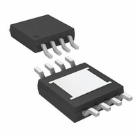
LTC3631IMS8E#TRPBF Linear Technology, LTC3631IMS8E#TRPBF Datasheet - Page 14

LTC3631IMS8E#TRPBF
Manufacturer Part Number
LTC3631IMS8E#TRPBF
Description
IC CONV STP-DWN SYNC ADJ 8-MSOP
Manufacturer
Linear Technology
Type
Step-Down (Buck)r
Datasheet
1.LTC3631EMS8E-5PBF.pdf
(22 pages)
Specifications of LTC3631IMS8E#TRPBF
Internal Switch(s)
Yes
Synchronous Rectifier
Yes
Number Of Outputs
1
Voltage - Output
0.8 ~ 45 V
Current - Output
100mA
Voltage - Input
4.5 ~ 45 V
Operating Temperature
-40°C ~ 125°C
Mounting Type
Surface Mount
Package / Case
8-MSOP Exposed Pad, 8-HMSOP, 8-eMSOP
Lead Free Status / RoHS Status
Lead free / RoHS Compliant
Power - Output
-
Frequency - Switching
-
Available stocks
Company
Part Number
Manufacturer
Quantity
Price
applicaTions inForMaTion
LTC3631
The minimum value of these thresholds is limited to
the internal V
Electrical Characteristics table. The current that flows
through this divider will directly add to the shutdown,
sleep and active current of the LTC3631, and care should
be taken to minimize the impact of this current on the
overall efficiency of the application circuit. Resistor values
in the megohm range may be required to keep the impact
on quiescent shutdown and sleep currents low. Be aware
that the HYST pin cannot be allowed to exceed its absolute
maximum rating of 6V. To keep the voltage on the HYST
pin from exceeding 6V, the following relation should be
satisfied:
The RUN pin may also be directly tied to the V
for applications that do not require the programmable
undervoltage lockout feature. In this configuration, switch-
ing is enabled when V
lockout threshold.
Soft-Start
The internal 0.75ms soft-start is implemented by ramping
both the effective reference voltage from 0V to 0.8V and the
peak current limit set by the I
To increase the duration of the reference voltage soft-start,
place a capacitor from the SS pin to ground. An internal
5µA pull-up current will charge this capacitor, resulting in
a soft-start ramp time given by:
When the LTC3631 detects a fault condition (input supply
undervoltage or overvoltage) or when the RUN pin falls
below 1.1V, the SS pin is quickly pulled to ground and the
internal soft-start timer is reset. This ensures an orderly
restart when using an external soft-start capacitor.
The duration of the 0.75ms internal peak current soft-start
may be increased by placing a capacitor from the I
to ground. The peak current soft-start will ramp from 50mA
to the final peak current value determined by a resistor
14
V
t
SS
IN(MAX)
= C
SS
•
IN
•
R1+ R2 + R3
0.8V
5µA
UVLO thresholds that are shown in the
R3
IN
surpasses the internal undervoltage
< 6V
SET
pin (50mA to 225mA).
IN
SET
supply
pin
from I
I
and ground, the peak current ramps linearly from 50mA
to 225mA, and the peak current soft-start time can be
expressed as:
A linear ramp of peak current appears as a quadratic
waveform on the output voltage. For the case where the
peak current is reduced by placing a resistor from I
to ground, the peak current offset ramps as a decaying
exponential with a time constant of R
case, the peak current soft-start time is approximately
3 • R
Unlike the SS pin, the I
ground during an abnormal event; however, if the I
pin is floating (programmed to 225mA peak current),
the SS and I
to a capacitor to ground. For this special case, both the
peak current and the reference voltage will soft-start on
power-up and after fault conditions. The ramp time for
this combination is C
Efficiency Considerations
The efficiency of a switching regulator is equal to the output
power divided by the input power times 100%. It is often
useful to analyze individual losses to determine what is
limiting the efficiency and which change would produce
the most improvement. Efficiency can be expressed as:
where L1, L2, etc. are the individual losses as a percentage
of input power.
Although all dissipative elements in the circuit produce
losses, two main sources usually account for most of
the losses: V
operating current dominates the efficiency loss at very
low load currents whereas the I
efficiency loss at medium to high load currents.
1. The V
SET
Efficiency = 100% – (L1 + L2 + L3 + ...)
The DC supply current as given in the electrical charac-
teristics and the internal MOSFET gate charge currents.
t
SS(ISET)
pin. With only a capacitor connected between I
ISET
SET
IN
• C
to ground. A 1µA current is sourced out of the
operating current comprises two components:
SET
= C
ISET
IN
operating current and I
ISET
pins may be tied together and connected
.
•
SS(ISET)
0.8V
1µA
SET
pin does not get pulled to
• (0.8V/6µA).
2
R loss dominates the
ISET
2
R losses. The V
• C
ISET
. For this
3631fc
SET
SET
SET
IN


